This is a superseded page, so you may want to look instead at the
superseding page instead of this one. On the other
hand ....
At the time the Virtual AGC electronic-simulation framework
and this explanatory page were first written, the simulation
framework was based on the file formats used by the KiCad
5 EDA system. But when KiCad 6 was subsequently
released (the stable version at this writing is 8), those file
formats were replaced by completely-different formats, thus
breaking the Virtual AGC electronic simulations at the same
time. This page relates to those still-available KiCad
5 based files, whereas the superseding page relates to the KiCad
6 (and beyond) simulation framework. This page could
nevertheless remain useful, and hence will be retained.
But this page is essentially a draft that was never perfected,
and therefore has some deficiencies even beyond its limitation to
KiCad 5.
One such deficiency is that setup is never discussed. I
would suggest using the superseding page's setup instructions.
Additionally, you will need to work within the superseded
"schematics-KiCad-5" branch of the Virtual AGC software repository
rather than the "schematics" branch that's advised in superseding
setup. In other words, you need to use schematic-diagram
files in their old formats rather than in their new ones.
Personally, I have both branches of the repository installed on my
computer, in separate folders, to have both available to me
simultaneously. My suggestion would be to install the old
files in a new folder called
"virtualagc-schematics-KiCad-5". Here's how to do that:
git clone --depth=1 -b schematics-KiCad-5 https://github.com/virtualagc/virtualagc.git virtualagc-schematics-KiCad-5
Any instructions that mention a folder such as Schematics/ are
referring to virtualagc-schematics-KiCad-5/Schematics/.
But because the installation instructions asked you to add the
virtualagc-schematics/Scripts/ folder to your PATH, we have a
slight problem with superseded framework, because it uses scripts
of the same names but stored in a different folder, namely
virtualagc-schematics-KiCad-5/Scripts/. In other words,
without further action on our part, we'd be in jeopardy of having
the normal, non-workaround scripts found rather than the KiCad 5
workaround scripts, which wouldn't do at all. To get around
this in Linux or Mac OS, I'd suggest doing this:
cd path/to/virtualagc-schematics-KiCad-5/Schematicsexport PATH=/absolute/path/to/virtualagc-schematics-KiCad-5/Scripts:$PATHcd \path\to\virtualagc-schematics-KiCad-5\Schematicsset PATH=\absolute\path\to\virtualagc-schematics-KiCad-5\Scripts;%PATH%Digital simulation of the AGC electrical design can provide
very-detailed insight into how that electrical design
functions. Aside from satisfying simple personal interest,
this is very valuable if you wish to create a simulation of the
AGC, in the manner of Virtual AGC Project's Block II AGC
software simulator or Block I
AGC software simulator, or John Pultorak's Block
I
AGC hardware simulator, and want to have some way of
verifying that your creation works properly.
Realize, though, that the purpose of these simulations can only
be very accurate examination or verification of behavior. At
the present time, these simulations are very much slower than real
time, so you cannot expect to use them as replacements for the
software simulations of the AGC CPU mentioned in the preceding
paragraph. One day, as computer speeds continue to advance,
perhaps! But not now.
The basic simulation process, from end to end, can be summarized
as follows:
Steps #1, #2, and #3, and creation of a simple test bench for
step #4, have already been accomplished for you by the Virtual AGC
Project. It only remains for you to modify the test bench,
select whichever AGC software you want to run on the simulation,
recompile the simulation, run the simulation, and look at the
results. Developing the test bench is the only tricky part.
Multiple types of simulation are possible, including:
Indeed, if you are capable of writing your own Verilog
descriptions of peripheral hardware in the LM or CM, you can
probably even simulate AGC+DSKY+Other. What we'll
concentrate on discussing, however, is the full AGC.
Hopefully, with that background, you'll be able to see for
yourself how to create and run some other granularity of the
simulation.
One slight point of confusion is that in the AGC design, the
various plug-in circuits are called "modules", while Verilog also
uses the term "modules" for its constructs that are similar to
"functions" or "subroutines" in other programming languages.
Now as it happens, we've implemented the simulation in such a way
that each AGC module actually is modeled as a single
Verilog module. That's more-or-less a coincidence, though,
and if you attempt to work with any simulations that differ from
those we've pre-prepared for you, you may have to watch out for
the dual meaning of this term.
The Virtual AGC Project's
Electro-Mechanical page.
Apollo-era AGC/DSKY electrical-schematic diagrams:
Open-source software:
Mike Stewart's similar transcription + simulation effort:
It should be noted that while the AGC simulations described on
this page were not based on Mike Stewart's pre-existing
project, Mike's simulation was a very important resource in the
sense that cross comparisons of the Mike's implementation with
this one provided a way to detect errors in both implementations
that would not have been easily discoverable otherwise.
The Virtual AGC software repository already contains some
fully-worked out examples of digital simulations. The simplest is
something called "testVerilog", which is actually a small circuit
block from the AGC's circuit module A1, the "scaler" module.
Let's consider the testVerilog simulation, within the context of
steps #1 through #7 outlined in the Introduction
above.
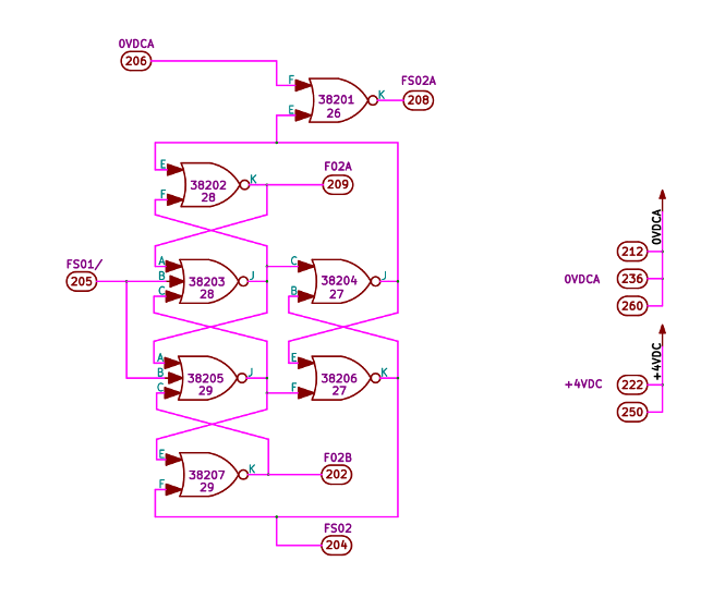
Step #1: Start with the original Apollo Program
schematic-diagram drawing for module A1, which is drawing
2005259A, two sheets (click to enlarge):
Don't be confused by the fact that the inputs of NOR gates in the
circuit are decorated with little triangles that make the gate
look like a rocket ship. They're just regular NOR gates in
spite of that. The numbered oval pads are the inputs from or
outputs to the AGC backplane.
After conversion to CAD, KiCad files for this circuit module are
here,
but for exposition purposes I've printed them out as simple images
as well:


Now, AGC module A1 is the "scaler" circuit. If you want to
read about it in some detail, you can look at section
4-5.3.4
of document ND-1021042, which covers the theory of operation
of this module. The module's purpose is to take clock signal
called FS01/ (a 102.4 KHz square wave), which you can see coming
into the module from the AGC's backplane near the upper left on
the first sheet of the schematic, and to run it through a sequence
of circuit blocks that successively cut the frequency of that
signal in half, as follows, and outputting those slower clocks
back to the AGC's backplane:
To simplify things, the testVerilog example cuts this all down so
that just the first divide-by-two circuit block, which produces
FS02 from FS01/, is retained in the design. The
CAD
files for testVerilog are here, but here is a simple image
of the circuit:
Step 2: Creation of a netlist from the CAD files. This is
just a feature of the KiCad program itself. While it isn't
terribly instructive, the netlist file for this circuit is
relatively short and relatively readable without any explanation,
so here it is in full:
Step #3: Conversion to Verilog. (You may have noticed that the Introduction mentions that at this point we need to specify the initial state of the flip-flops. If you are an electronics novice it may not be obvious, but to any experienced electronics designer it will have been obvious that the feedback between the pairs of NOR gates in the circuit does indeed create a flip-flop, or at least introduces some kind of memory. For our purposes at the moment, we'll just skip over that point, and note that the repository provides a file called module.init that specifies the initial conditions of the implicit flip-flop. Besides that, another input file called pins.txt is needed, which again, we'll just accept for the moment without further explanation.)
( { EESchema Netlist Version 1.1 created  Wed 26 Sep 2018 08:21:48 AM CDT }
( /5D281B38 $noname  J2 ConnectorA1-200
(  202 Net-(J2-Pad202) )
(  204 Net-(J2-Pad204) )
(  205 Net-(J2-Pad205) )
(  206 Net-(J2-Pad206) )
(  208 Net-(J2-Pad208) )
(  209 Net-(J2-Pad209) )
(  212 0VDCA )
(  222 +4VDC )
(  236 0VDCA )
(  250 +4VDC )
(  260 0VDCA )
)
( /5D281B3E $noname  U126 D3NOR-+4VDC-0VDCA-A_B-E_F
(    6 0VDCA )
(    7 Net-(U126-Pad7) )
(    8 Net-(J2-Pad206) )
(    9 Net-(J2-Pad208) )
)
( /5D281B45 $noname  U128 D3NOR-+4VDC-0VDCA-ABC-E_F
(    1 Net-(U127-Pad2) )
(    2 Net-(U127-Pad8) )
(    3 Net-(J2-Pad205) )
(    4 Net-(J2-Pad209) )
(    5 0VDCA )
(    6 0VDCA )
(    7 Net-(U126-Pad7) )
(    8 Net-(U127-Pad2) )
(    9 Net-(J2-Pad209) )
(   10 +4VDC )
)
( /5D281B77 $noname  U127 D3NOR-+4VDC-0VDCA-B_C-E_F
(    1 Net-(U126-Pad7) )
(    2 Net-(U127-Pad2) )
(    3 Net-(J2-Pad204) )
(    4 0VDCA )
(    5 0VDCA )
(    6 0VDCA )
(    7 Net-(U126-Pad7) )
(    8 Net-(U127-Pad8) )
(    9 Net-(J2-Pad204) )
(   10 +4VDC )
)
( /5D281B9B $noname  U129 D3NOR-+4VDC-0VDCA-ABC-E_F
(    1 Net-(U127-Pad8) )
(    2 Net-(J2-Pad202) )
(    3 Net-(J2-Pad205) )
(    4 Net-(U127-Pad2) )
(    5 0VDCA )
(    6 0VDCA )
(    7 Net-(U127-Pad8) )
(    8 Net-(J2-Pad204) )
(    9 Net-(J2-Pad202) )
(   10 +4VDC )
)
)
*
Step #4: Creation of a test bench. This is the point in a real simulation task where you would have to decide what it is you want from the simulation, and write a test bench file in Verilog to provide the appropriate inputs at the proper time to do the testing you have in mind. For the purpose of this example, though, we've simply provided a test-bench file, which looks like this:// Verilog module auto-generated for AGC module A1 by dumbVerilog.py module A1 ( rst, FS01_, F02A, F02B, FS02, FS02A ); input wire rst, FS01_; output wire F02A, F02B, FS02, FS02A; assign FS02A = rst ? 0 : ~(0|U126Pad7); assign FS02 = rst ? 0 : ~(0|U126Pad7|U127Pad8); assign U127Pad8 = rst ? 1 : ~(0|F02B|FS01_|U127Pad2); assign U126Pad7 = rst ? 1 : ~(0|U127Pad2|FS02); assign U127Pad2 = rst ? 0 : ~(0|U127Pad8|FS01_|F02A); assign F02A = rst ? 0 : ~(0|U126Pad7|U127Pad2); assign F02B = rst ? 0 : ~(0|U127Pad8|FS02); endmodule
// Test bench for testVerilog.v
`timescale 1us / 1ns
module testVerilog;
reg rst = 1;
initial begin
$dumpfile("testVerilog.vcd");
$dumpvars(0, testVerilog);
# 2 rst = 0;
# 500 $finish;
end
reg FS01_ = 0;
always #4.883 FS01_ = !FS01_;
wire F02A, F02B, FS02, FS02A;
A1 A1A (
rst, FS01_, F02A, F02B, FS02, FS02A
);
initial
$timeformat(-6, 0, " us", 10);
initial
$monitor("At time %t, rst=%d, FS01_=%d, F02B=%d, FS02=%d, FS02A=%d, FS02A=%d", $time, rst, FS01_, F02B, FS02, F02A, FS02A);
endmodule
Let's take a look at this file and see what it says. First,
the "timescale" directive explains how to understand the timings
(the things marked with "#") that appear within the test-bench
file. It says that the time scale will be 1 us, so that the
numbers for the "#" timings are in microseconds. VCD info: dumpfile testVerilog.vcd opened for output.Thus as promised, FS01/ toggles about very 5 microseconds, while FS02 toggles about every 10 microseconds.
At time 0 us, rst=1, FS01_=0, F02B=0, FS02=0, FS02A=0, FS02A=0
At time 2 us, rst=0, FS01_=0, F02B=0, FS02=0, FS02A=0, FS02A=0
At time 5 us, rst=0, FS01_=1, F02B=1, FS02=0, FS02A=0, FS02A=0
At time 10 us, rst=0, FS01_=0, F02B=0, FS02=1, FS02A=0, FS02A=1
At time 15 us, rst=0, FS01_=1, F02B=0, FS02=1, FS02A=1, FS02A=1
At time 20 us, rst=0, FS01_=0, F02B=0, FS02=0, FS02A=0, FS02A=0
At time 24 us, rst=0, FS01_=1, F02B=1, FS02=0, FS02A=0, FS02A=0
At time 29 us, rst=0, FS01_=0, F02B=0, FS02=1, FS02A=0, FS02A=1
At time 34 us, rst=0, FS01_=1, F02B=0, FS02=1, FS02A=1, FS02A=1
At time 39 us, rst=0, FS01_=0, F02B=0, FS02=0, FS02A=0, FS02A=0
At time 44 us, rst=0, FS01_=1, F02B=1, FS02=0, FS02A=0, FS02A=0
At time 49 us, rst=0, FS01_=0, F02B=0, FS02=1, FS02A=0, FS02A=1
At time 54 us, rst=0, FS01_=1, F02B=0, FS02=1, FS02A=1, FS02A=1
At time 59 us, rst=0, FS01_=0, F02B=0, FS02=0, FS02A=0, FS02A=0
At time 63 us, rst=0, FS01_=1, F02B=1, FS02=0, FS02A=0, FS02A=0
At time 68 us, rst=0, FS01_=0, F02B=0, FS02=1, FS02A=0, FS02A=1
At time 73 us, rst=0, FS01_=1, F02B=0, FS02=1, FS02A=1, FS02A=1
At time 78 us, rst=0, FS01_=0, F02B=0, FS02=0, FS02A=0, FS02A=0
At time 83 us, rst=0, FS01_=1, F02B=1, FS02=0, FS02A=0, FS02A=0
At time 88 us, rst=0, FS01_=0, F02B=0, FS02=1, FS02A=0, FS02A=1
At time 93 us, rst=0, FS01_=1, F02B=0, FS02=1, FS02A=1, FS02A=1
At time 98 us, rst=0, FS01_=0, F02B=0, FS02=0, FS02A=0, FS02A=0
...
At time 498 us, rst=0, FS01_=0, F02B=0, FS02=1, FS02A=0, FS02A=1
Step #7: Visualization. When the dump-file created by running the simulation, namely testVerilog.vcd, is pulled into the GTKWave visualization program, you see something like the following. The picture doesn't seem to require any explanation, though it's fun to compare it to the corresponding picture on p. 4-222A of document ND-1021042.
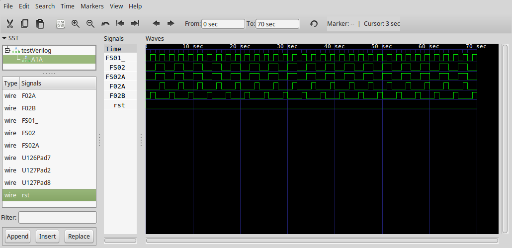
Aside: Simulation-result dumpfiles can be in a number of file-formats, with designations like VCD, LXT2, FST, and so on. You many notice that in the screenshot above, the simulation dumpfile is called "module.fst" rather than the "testVerilog.vcd" as the descriptive text above claims. A mixup on my part, I suppose! At any rate, the data depicted is what the text says it is!
For our discussion (and in our
repository for electrical schematics and Verilog descriptions of
them), we expect a certain directory hierarchy and
file-naming convention within that hierarchy. It looks like
this:
Top level directory of the repository/The items in green above are the ones that are either provided for you in our repository or are created more-or-less automatically for you by the process that will be described later on. The items in reddish-brown above may be partially created for you to give you a head start, but nevertheless require some active involvement on your part to get them just right, in those cases where you actually need the files. But in brief, the electrical design for any given part number of the AGC (such as 2003200 or 2003993) consists of a set of drawings of the individual circuit modules, plus the "backplane", i.e. the set of electrical interconnections between the modules. For AGC p/n 2003200, for example, those items are implemented by the Verilog files:
Scripts/
dumbVerilog.pySchematics/
dumbTestbench.py
roms/
Artemis072.v
Aurora12.v
...
Validation.v
Validation-hardware-simulation.v
DRAWING1/
DRAWING2/module.net
- ... schematics ...
module.init
tb.v
module.v
module_tb.v
module.vvp
... schematics ....
module.net
module.init
tb.v
module.v
module_tb.v
module.vvp
.
.
Makefile
2003200.v
tb-2003200.v
2003200.vvp
2003993.v
tb-2003993.v
2003993.vvp
.
.
.
Since this is something that has already been done for you, and
the repository has these files in it, there's not much you need to
know about it. So (lucky you!) I'm not actually going to
describe how to perform these steps.
However, here are some basic factoids that may or may not be of
interest:
The AGC's logic module circuits, modules A1-A24
mostly consist of so-called "combinational" logic, in which a
unique set of inputs determines a unique set of outputs at any
specific moment of time. However, some of the NOR gates,
such as those in the figure to the left (which is from the testVerilog example
given earlier), contain feedback in which the inputs to a NOR gate
may depend indirectly on its output. The net result is for
those portions of the circuit to have a kind of "memory", in which
the current output depends not just on the inputs at this precise
moment in time, but also on the inputs at earlier times as well.
When confronted with a situation like this, the Verilog simulator
software may not be able to initially figure out what the outputs
of the circuit are, because those depend on times before the
simulation started, about which the simulator software has no
information. In real life, such as in the real physical
AGC units, those circuits will settle very quickly into some
stable state. But in simulation that may not be the case,
and the circuit may oscillate endlessly. So we have to have
some way to initially get the system into some stable state in
which all of the feedback signals have some nice, consistent
values.
 The way that is done is with module.init
files. Each schematic drawing needs to have one of
these. A module.init file can provide settings for any or
all of the NOR gates, driving their outputs to a desired state
when a signal ("rst") is initially applied to the circuit.
The way that is done is with module.init
files. Each schematic drawing needs to have one of
these. A module.init file can provide settings for any or
all of the NOR gates, driving their outputs to a desired state
when a signal ("rst") is initially applied to the circuit.
Before describing the format of the module.init files, though, we
need to agree on some basic facts about the NOR gates used in the
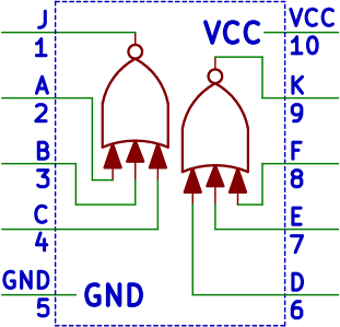
AGC circuits. The NOR gates are packaged into 10-pin
integrated circuits, each of which contains two independent NOR
gates, as in the figure to the right. One of the NOR-gates
outputs to the chip's pin 1 (called "J") on the schematics, while
the other NOR-gate outputs to pin 9 (or "K").
The other thing to notice is that, as in the figure to the left,
the dual NOR-gates are identified in the Verilog design by
reference designators like U1nn, U2nn, or U3nn,
where nn is a 2-digit number written on the NOR-gate's
schematic symbol. In the figure at left, for example, we
have both NOR gates from U127, both NOR gates from U128, both NOR
gates from U129, and one of the two NOR gates from U126. How
did I know that we had U127 rather than U227? Well, usually
U1nn is on the first sheet of the schematic and U2nn
is on the second sheet. However, to know for sure, you
really need to read the textual notes provided within the
schematic.
With those understandings in mind, here's a portion of a
module.init file for your consideration. (It does not
belong to the example figure above.)
# For module A2
U151 1 0 0.2
U152 0 0 0.2
U153 0 0 0.2
U155 1 0 0.2
U156 0 0 0.2
U157 1 0 0.2
U308 0 0
U309 0 0
U228 1 0
...
You can decorate the module.init file with comments (preceded by
"#") or blank lines, if it helps you document what's being
done. More importantly, the file can be edited in a
text-editor and consists of lines of the form
Unnn [ JVALUE [ KVALUE [ JDELAY [ KDELAY ]]]
by which I mean that the lines consist of the chip's reference
designator, follow by 0 to 4 numerical values. JVALUE and
KVALUE are simply the values of the NOR gates' outputs at
reset, and always have the settings 0 or 1. 0 is the
default, meaning that the output of the NOR is LOW.
How does one determine what values JVALUE and KVALUE
should be given? What you are looking for, minimally, is
that all of the outputs from the NOR gates should be consistent
with their inputs. You know that that's possible, since the
original AGCs didn't simply oscillate out of control, But
how?
One way is to use a handy script we've provided,
Scripts/dumbInitialization.py, which I describe in more detail in
the Appendix.
This was the method used to create the module.init files presently
in the repository. But if the initializations created this
way don't satisfy you, you can edit them according to your own
liking, because they're just text files. It is certainly a
drawback of dumbInitialization.py that the initializations aren't
necessarily "natural", since the only guarantee is that they are
mutually consistent rather than to have any other properties you
might like. For example, module A1 is basically just a
33-bit counter, and that counter is initialized to some "random"
value by dumInitialization.py, whereas you might like it
to be initialized to 0. I fear that's just a consequence of
how the flip-flops were implemented in the AGC, as there's nothing
(as far as I know) that guarantees how they're initialized.
And sadly, I have nothing other than that smug platitude to offer
you about creating your own custom initializations.
What are JDELAY and KDELAY? Well, they have
to do with a completely different topic. The Verilog
description of the design allows you to assign any gate delay you
like to any of the NOR gates. Mostly it isn't critical, and
the default we use is a delay of 0. But in some cases it is
critical that it be non-zero, or even that it is confined within a
narrow range of acceptable values. The units of time are
defined by the "timescale" operative that appears near the top of
many of the Verilog files. Usually this is 100 ns per
simulator timer tick. Therefore, for example, a JDELAY
or KDELAY of 0.1 would be 10 ns.
A "test bench" is a Verilog file that lets you define how to
stimulate the inputs of the Verilog file(s) for an individual AGC
module or combination of AGC modules, and therefore to produce
outputs that you can either view immediately or log for later
analysis/viewing. When you compile the Verilog file for the
test bench along with the Verilog file(s) it is the test bench
for, you get a file that can be used to simulate the design
without further ado.
Unfortunately, I cannot tell you much about how to write Verilog
test-bench files, since it's going to depend so much on the
particular AGC p/n or AGC module or PCB you're trying to test, and
what you're trying to test within it. You'll simply have to
research these topics for yourself.
I will tell you that the software repository does have template
testbench files (produced by the script dumbTestbench.py as
described in the preceding section) that you can use as starting
points, or else completely-working testbench files in a few cases,
wherever it makes sense in the present state of development to do
so:
Alas! there's one point in the simulation where we depart
somewhat from absolute verisimilitude with respect to the original
AGC circuitry, and that's in the simulation of the AGC's erasable
memory (the "RAM") and fixed memory (the "ROM"). Because the AGC's
memory was made from Permalloy-wire cores, surrounded by lots of
analog circuitry to drive them and to sense their states, it
becomes a bit tricky to simulate their behavior in essentially
digital simulation tools like Icarus Verilog.
What's done in the simulation instead is to continue to use the
digital signals that the AGC feeds into the analog circuitry
driving the cores or extracts from the analog circuitry sensing
the cores, but to replace the cores themselves and their
surrounding analog circuitry with a
fully digital model whose schematics and associated Verilog can
be found in the github repository. Specifically, the
fixed memory ends up being modeled
after a Microchip SST39VF200A flash-memory chip (Verilog
module ROM.v), not that the choice of this specific part has too
much significance, as long as it has sufficient capacity. As
far as the contents of the memory are concerned, it can be
any of the AGC programs available to us in the Virtual AGC
project: Artemis 072, Aurora 12, Colossus 237, etc.
It's only necessary to make sure that the particular Verilog file
implementing the desired AGC program is present in the
Schematics/roms/ folder at compile time, and is named
"rom.v". For convenience, each
of the available AGC programs has been converted into the form
needed for the Verilog to use them, and can be selected at
the time the Verilog is compiled (see the next section).
It is worth noting, though, that the simulation of the
electronics runs very slowly relative to real time, and
that there isn't presently any way to model an interactive DSKY in
the simulation, so the choice of which AGC programs to use is
really limited greatly by which of them are easy to use,
pragmatically speaking. The AGC program called
"Validation-hardware-simulation" is one such program: it has been
modified to operate without DSKY input, and only require about 40
seconds to run in real life. In the simulation, it requires
much, much more time.
But if you're running Windows or just want to know how to do the
steps yourself, that doesn't really help you too much.
(Unless somebody wants to fix up a Windows version of the Makefile
for me? It shouldn't be too hard, but I don't want to mess with
Windows myself, so it's left as an exercise for the reader.)
For you folks, here's how the compilation step works.
There are really two cases of interest. First, you might
want to simulate a single AGC module, to exercise its functions
and perhaps to debug it. For concreteness, let's imagine
that this module has drawing number 2005123A, and hence its files
reside in the directory Schematics/2005123A. There will be
two relevant files in that directory: module.v, which is the
Verilog of the module itself, automatically translated from the
CAD files for drawing 2005123A, and module_tb.v, the Verilog file
of the "test bench" of the module. As explained earlier,
there will be either an automatically-generated version of the
test bench or else a manually tweaked version of the test bench
file already in place. But it's up to you to insure that the
test bench does what you want. The compilation is simple:
cd Schematics/2005123A
iverilog -o module.vvp module_tb.v module.v
which produces an object file, Schematics/2005123A/module.vvp.
The second case is simulation of a complete AGC unit. Let's
suppose that this is the AGC with p/n 2003200. AGC p/n is
essentially a collection of various AGC modules, plugged into a
"backplane". Module A1 is drawing 2005259A, module A2 is
drawing 2005260A, etc., up through module A24, drawing
2005273A. As above, there is a testbench file, 2003200.v,
which represents the backplane, along with any stimulation you
need to apply to the backplane symbols, and any probing you need
to do on those signals. So here is what the Verilog
compilation looks like:
cd Schematics
iverilog -o 2003200.vvp 2003200.v 2005259A/module.v 2005260A/module.v ... 2005273A/module.v
This produces an object file, Schematics/2003200.vvp.
cd Schematics/2005123Awhile to simulate AGC p/n 2003200 we'd do this:
vvp module.vvp
cd SchematicsDepending on your intentions — i.e., how the testbench is written — the simulation may or may not be a hands-off operation. Typically, though, it would result either in messages printed out to the terminal or creation of a log file for later viewing and analysis, or both.
vvp 2003200.vvp -lxt2
Assuming that your simulation produces a log file for later
viewing or analysis, there are several choices.
For example, as mentioned in the preceding section, a VCD log
file is ASCII, and therefore very suited for some kind of
post-processing with scripts written in AWK or Python or some
other language.
Often, though, it's nicer to just view some set of signals of
interest as if using an oscilloscope or logic analyzer. A
program like GTKWave is great for this, in that it can view either
VCD or LXT2 files, and you can select the specific signals you
want to view, and the ordering of those signals. For the
examples we've been using, you'd do one of the following and then
just monkey around in GTKWave's GUI:
cd Schematics/2005123A
gtkwave module.vcd
or
cd Schematics
gtkwave 2003200.lxt2
cd Schematicsor perhaps
make
cd SchematicsIf you're a bit less lucky, you'd probably have to run our netlist-to-Verilog translation script manually. This is the Python 3 script Scripts/dumbVerilog.py, and taking into account our directory and file-naming conventions, you'd do this:
make clean all
cd Schematics/DRAWING_NUMBERThe only things that really need to be filled in here are the AGC MODULE number (A1, A2, ..., A24) and the default gate DELAY. The unit in which DELAY is expressed ultimately depend upon the time-scale that will eventually be set in the test bench. Now, the basic AGC clock speed is 1.024 MHz, but the simulation cycle time must then be 2.048 MHz, since that's the rate at which the clock toggles. For this reason, all test bench Verilog automatically produced (see the next section) uses a basic time-scale of 100 ns. The nominal gate delay of AGC NOR gates was 20 ns., so that means a reasonable DELAY might be 0.2, and therefore that's what we typically use.
../../Scripts/dumbVerilog.py MODULE module.net ../..Scripts/pins.txt DELAY module.init >module.v
A consistent set of flip-flop initializations can conveniently be
generated using the Python 3 script
Scripts/dumbInitialization.py. If you are running Linux then
the simplest thing to do (for, say, AGC model 2003200) is just
cd Schematics
make clean all
make 2003200.init
make clean all
Of course, if you don't have Linux then this doesn't help you too
much, so let's consider how to go about generating the flip-flop
initialization files (DRAWING/module.init) as a manual
operation rather than using the handy-dandy Makefile. The
basic syntax is simply
dumbInitialization.py <INPUT.v
However, this simple statement hides some inconvenient
complexity. Using dumbInitialization.py to create an
initialization file requires having the Verilog for the circuit at
hand, whereas generating the Verilog for the circuit requires
having the initialization file at hand! Fortunately, this
circle is not as vicious as it appears, since all you really have
to do is this:
That's why in the Makefile example we started with, there are two
"make clean all" steps.
There are two basic scenarios for which you'd want to generate
initialization files, I think: You might want an
initialization file for an AGC module considered as a stand-alone
unit. Or, you might want an initialization file for the
complete set of AGC modules of a given AGC part number. The
latter has an advantage over the former, in that the
initialization is internally consistent throughout the entire
AGC. Besides, an initialization file of the full-AGC type
works perfectly well for an individual module, but not
vice-versa. So let's assume you really want initialization
files for the AGC as a whole.
The first step, of course, is to take all of the Verilog files
for the individual AGC modules, and concatenate them to form one
large file. For AGC model 2003200, for example, those files
are 2005259A/module.v, 2005260A/module.v, ...,
2005273A/module.v. (The drawing numbers for the AGC modules,
which is essentially what these are, are listed both on the Electro-Mechanical page of
the website, and in Schematics/Makefile.) You can combine
these files, for example, using a text-editor program. The
second step is to actually run dumbInitialization.py:
Scripts/dumbInitialization.py < BigCombinedVerilogFile.vThe result is the creation of files files A1.init, A2.init, ..., A24.init. These need to be copied into the appropriate drawing directories and be renamed to module.init. For example, A1.init might become 2005259A/module.init.
Scripts/dumbTestbench < BigCombinedVerilogFile.v > Testbench.vSuch a testbench probably still needs considerable tweaking, but it's a good place to start.