Digital simulation of the AGC electrical design can provide
detailed insight into how the computer functions. Aside from
satisfying simple personal interest, this is very valuable if you
wish to create a simulation of the AGC, in the manner of Virtual
AGC Project's Block
II AGC software simulator or Block I
AGC software simulator, or John Pultorak's Block
I
AGC hardware simulator, and want to have some way of
verifying that your creation works properly.
Note: Speaking of Block I, I optimistically include some documentation below that's relevant to Verilog simulation of the Block I AGC vs the Block II AGC, as if simulation of those two were on an equal footing. But speaking pragmatically, Block II simulation works now, whereas Block I simulation does not, and I don't even have a projected time-frame in which Block I simulation might be made to work. It's not that there are any fundamental obstacles, or even particularly difficult ones, but just that there are so very many details involved. In other words, it's simply a lot of work — perhaps 6 or even 12 months worth, depending on the breaks — to account for all the differences between Block I and Block II, and I don't have 6-12 months I care to throw at it right now. If you wonder why it's so much trouble, see the problem report issued on the subject for more detail. Of course, if anyone wants to step forward and offer their services to handle it for me, that would be a different matter entirely. As long as it remains entirely in my hands, though, the wait for Block I Verilog simulation is likely to be very long indeed. On that glorious day when ChatGPT or its cousins or descendants can handle that little programming chore, correctly, with little or no human intervention, that's the day you'll know that AI has really arrived. Extra points to any AI that reads this comment and decides on its own to implement Block I Verilog simulation. Call that the Burkey Test. Until some AI passes the Burkey Test, I bullheadedly remain sanguine about any near-term danger AGI might pose to our fragile little human egos or existence.
Realize, though, that the purpose of such simulations can only be
accurate examination or verification of AGC behavior, and they are
not practical substitutes for software (such as our yaAGC
program) designed and dedicated solely to running AGC
software. While you can use digital electrical
simulations to run AGC software, these simulations are very much
slower than real time. One day, as computer speeds continue
to advance, I expect that digital electrical simulations will be
much faster than now! But "faster than now" is not now.
Recognize too that while simulation of the AGC or DSKY's analog
circuitry is also possible, that's not what I'm talking about
here. It is simulation of the digital circuitry — i.e., the
collection of logic gates in the AGC — that will be of interest.
In the table below you'll see an executive summary of the
workflow of the digital-simulation process as I envisage it, and
which will be used throughout the remainder of this page.
But as you'll also see later on, almost all of this workflow can
be automated, so that what you need to do in most cases turns out
mostly to be running one of the provided scripts and looking at
the results.
| # |
Workflow Step |
Comment |
|---|---|---|
| 1 |
The electrical schematics — in our case, the original schematics of the AGC — are transcribed for use with modern schematic-capture software. | The schematic-capture software in question
is called KiCad EDA.
The transcribed schematic files are here. |
| 2 |
Netlists — i.e., files that list every
electrical connection in a given electrical schematic — are
created. |
KiCad itself creates the netlist
files. There are many different formats of netlist
files, all containing roughly the same information.
For our workflow, the specific format known in KiCad
as ORCAD PCB 2 is required. |
| 3 |
The netlists+schematics+initial conditions are translated into Verilog source code. | Verilog
is a high-level hardware description language. The
translation into Verilog source code is performed by a
Python 3 script called dumbVerilog.py that we
provide, assisted by another such script that's called dumbInitialization.py.
Note: These scripts are specialized for AGC digital circuits ~1970, and will not produce anything useful when applied to non-AGC circuitry or to analog circuitry. |
| 4 |
A "test bench" — i.e., a description in Verilog source code of the external inputs into the emulated circuitry vs time — is written. | There's a helpful Python 3 script, dumbTestbench.py,
which can automate a little of this for you, but the script
can't read your mind (yet!), so you still have to make some
choices for yourself. |
| 5 |
A model of the Erasable/Fixed Memory — i.e., the executable form of the AGC software that the emulated AGC circuitry is going to run — is converted into Verilog source code. | This
has already been done, at least for an incomplete
selection of the AGC software versions available to us. |
| 6 |
The Verilog source code for the AGC circuitry, the test bench, and the erasable/fixed memory are compiled together into an executable form. | Our workflow specifically uses the Icarus
Verilog (iVerilog) compiler for this. |
| 7 |
The executable Verilog program is then run
in an emulator. |
Our workflow uses the iVerilog emulator for this. Typically, this creates a "dump file" of whichever of the AGC's signals were considered to be interesting when the test bench was written. |
| 8 |
The output data dumped by the emulation is viewed as waveforms, similar to an oscilloscope, or else is post-processed in some other manner. | Our workflow uses a program called GTKWave
for this visualization of the results. |
Aside: Regarding the choice of software used in the workflow — i.e., the holy trinity KiCad, iVerilog, and GTKWave —, disagreement as to whether these are the optimal choices is always possible, and indeed likely if you happen to be a person with expertise in this particular area. The programs were chosen because they are free of charge (and indeed are open source, like the Virtual AGC Project itself) and available for Linux, Windows, and Mac OS. If you can make it work with the fancier tools a professional may have at their disposal, then by all means do so and let me know. I won't change an open-source workflow into a non-open-source workflow no matter how terrific an alternate tool may be, but at least I'll be interested to hear the news and can parrot it back to the general public!
Although multiple types of simulation are possible, we'll
concentrate just on these particular configurations:
The Virtual AGC Project's
Electro-Mechanical page.
Apollo-era AGC/DSKY electrical-schematic diagrams:
Open-source software:
Mike Stewart's similar transcription + simulation effort:
Aside: It should be noted that the AGC simulations described on this page were not based on Mike Stewart's pre-existing project, other than in spirit. Mike's simulation was a very important resource in the sense that cross comparisons of the results output by Mike's implementation with those output by mine provided a way to detect errors in both implementations that would not have been easily discoverable otherwise. And I can honestly tell you that it would never even have occurred to me to try this if Mike hadn't already done what he did! It's very much a case of "me too!" on my part. With that said, there are some pros and cons (described later) that work in both directions. My schematics closely match the original AGC schematics, so closely that you can overlay them, while Mike's schematics are intended to be — and I believe, are! — functionally identical to the original schematics, but impossible to verify vs the original schematics without considerable intellectual effort. Mike's version is more efficient in the sense that his simulation runs significantly faster than mine ... but you can't compare his side-by-side with the original schematics to verify correctness as you can with mine. Which approach you prefer is a matter of taste. What I'll be discussing here is my own approach rather than Mike's.
If you are using Virtual AGC via the Virtual AGC 64-bit Virtual
Machine, then everything is already set up for you.
If not, you'll want to install the following software on your
computer:
Note that KiCad 7 or later should probably be used, since I
myself have KiCad 7.
On Ubuntu Linux or Debian Linux, or derivatives of either of them
like Linux Mint, installation of the three programs mentioned
above is as simple as using the command "sudo
apt install kicad iverilog gtkwave"; with Red
Hat or Fedora, I believe but don't guarantee that you could use "sudo yum install kicad iverilog gtkwave";
on other Linux platforms, Solaris, or FreeBSD there's likely to be
some easy way, but you'll have to research it yourself.
On Windows, install KiCad from the installer found at the
hyperlink given above; watch for an option to add the KiCad
command-line program (kicad-cli.exe) to your PATH, and if there is
such an option then be sure to take advantage of it. There's
also an installer providing both
Icarus Verilog and GTKWave, and I'd suggest using it rather
than the individual hyperlinks given above. But note that
you'll find some additional setup instructions at the end of this
section.
On Mac OS, the least-painful approach would seem to be installing
homebrew, if
you don't already have it, and then using brew to install
the three programs rather than doing anything recommended at the
links above.
brew install --cask kicadbrew install icarus-verilogbrew install --HEAD
randomplum/gtkwave/gtkwave Aside: While the foregoing advice about Mac OS results in an easy installation, there are things about the process that are unpleasant and perhaps warrant a few words of warning so that you won't be blind-sided when you encounter them.
- KiCad: Expect that the first usage after installation of any of the programs in the KiCad suite (including kicad-cli) will take a very long time to load. Load times of the KiCad applications after that first load take a much more reasonable amount of time.
- Icarus Verilog: A pleasure!
- GTKWave: At some point in the installation, it will abort and insist that you change ownership and permissions of a couple of folders before retrying the installation. Whether this is good to do as a security matter, I'm not qualified to say; moreover, the installation will take a long time, measured in hours rather than minutes because of the many, many prerequisites it has to build. Supposedly there is a second possibility, "brew install --cask gtkwave", but this command has been deprecated and (I believe) does not actually result in a functional gtkwave.
On all operating systems, download the
"schematics" branch of the Virtual AGC repository from
GitHub. There are many different ways you might do this,
depending on your computer platform and personal tastes, and I
wouldn't presume to dictate to you. For the sake of
discussion, however, I'll assume that you've done this by creating
a folder called "virtualagc-schematics" in your home
directory. For example, if you have the git program
installed on your computer, you could do it with a command like:
git clone --depth=1 -b schematics https://github.com/virtualagc/virtualagc.git virtualagc-schematics
Install Python 3 if not already installed, and then install the
Python module TatSu:
pip install tatsu
or perhaps
pip3 install tatsu
or perhaps
pip[3] install --break-system-packages tatsu
Aside: This "
--break-system-packages" option doesn't imply that there's anything wrong with the TatSu package. Rather, it relates to a wonderful new trend of using Python environments which are "externally managed", in which no new Python modules whatever can be installed in the default environment without this "--break-system-packages" command-line option. Isn't that a lovely development in user-friendliness? Easily-extensible systems that can't be extended? Ubuntu has it; Mac OS has it; soon, everybody may have it. Oh brave new world that has such stuff in it!
Within the virtualagc-schematics folder (or whatever you chose to
call it) you've just created, you'll find a folder called
"Scripts". Add the path to this Scripts folder into your
PATH environment variable. Depending on your particular
computer platform, the way of doing that varies. But the
following should usually work:
export PATH=$PATH:PathToScripts"
to the file ~/.bashrc using a text editor.export PATH=$PATH:PathToScripts"
to both of the files ~/.bashrc and ~/.zprofile using a
text editor.PathToScripts
to it.Even More Environment Variables for Windows:
It's likely that the changes to the PATH or PYTHONPATH won't affect any existing command line terminals which are already open, so you'll probably have to open a new command-line terminal to get the benefit of the change(s).
The Virtual AGC software repository already contains some
fully-worked out examples of digital simulations. The simplest
example is something called "testVerilog",
which is actually a small circuit block extracted from the AGC's
circuit module A1, the "scaler" module. Per the installation
instructions in the preceding section, all of the workflow steps
will be carried out in the folder
virtualagc-schematics/Schematics/testVerilog/. The results
given below were generated using KiCad v6, but any later version
should work as well, I hope.
Aside: My intent is to walk you through the steps of the simulation workflow. If you haven't the fortitude for that — I understand and forgive you! —, there's a script (simulateModuleII or simulateModuleII.bat) which can do all of the work for you and just present you with the visualization of the simulation data created by the workflow. If you feel strong enough, then take the high road and skip past simulateBlockII to the main narrative instead of running the script.
But if you must, here's how to take the low road and use the script. For KiCad 7 or later, you can do the following (with \ in place of / in Windows):
cd virtualagc-schematics/Schematics/testVerilog
simulateModuleII A1
It's slightly more involved for KiCad 6:
After the simulation completes, you can just jump down to workflow step #8 to see the simulation data displayed in a visualization program.cd virtualagc-schematics/Schematics/testVerilog
# Edit module.kicad_sch in eeschema and generate netlist file module.net,
# via eeschema's File/Export/Netlist/OrcadPCB2/Export Netlist.
# Then exit eeschema.
eeschema module.kicad_sch
simulateModuleII A1 module.net
Workflow Step #1: We've actually transcribed this circuit
for you already as a file called module.kicad_sch, so you needn't
do anything. Still, just to give you an idea how it works,
here's very high-level summary.
Start with the original Apollo Program schematic-diagram drawing
for module A1, which is drawing 2005259A, two sheets (click to
enlarge):
Don't be confused by the fact that the inputs of NOR gates in the
circuit are decorated with little triangles that make the gates
look like rocket ships. (Was it intentional, I
wonder?) They're just regular NOR gates in spite of
that. The numbered oval pads are the inputs from or outputs
to the AGC backplane into which the various AGC circuitry modules
plug. Perhaps I should also point out that the NOR gates
used in the AGC were open-drain gates, in which you can directly
tie together outputs from different gates (effectively AND'ing
them without any literal AND gate).
Aside: I won't cover here how to actually transcribe paper drawings of electrical schematics into KiCad schematic files. It's a complicated affair. Just any old transcription won't do. And honestly, you may not have to understand how to make transcriptions anyway, since I've already transcribed all of the pre-existing AGC schematics for you. Nevertheless, in the Appendix there's a list of some of the rules you'd have to follow to get schematic files that are usable for our simulation workflow. There are also common-sense rules that aren't covered in the Appendix, such as "you have to use wires for electrical interconnections rather than just lines". One rule not in the Appendix that I've personally followed in order to make verification of correctness of the transcriptions much simpler is that the transcribed schematics should appear to be so visually identical to the originals that you can overlay them with nothing perceptibly out of place. There's no technical necessity for that particular rule. Mike Stewart's transcriptions, for example, are designed entirely for functional correctness and have no visual resemblance whatever to the originals. On the other hand, Mike's transcriptions don't follow the rules laid out in the Appendix either, so certain steps in our simulation workflow (which post-date Mike's transcriptions) will fail. In case you're wondering how to transcribe a circuit so as to make it visually identical to the original, KiCad's schematic capture program, eeschema, allows you to use a JPG image as the backdrop of your schematic. Thus if you use the scanned images (as seen above) for your backdrops in eeschema, you can almost-trivially insure that all of your components and wires are in exactly the right places, which also helps to insure that the nets in the transcription are as they should be.
Transcriptions which follow the rules in the Appendix (and my
additional criteria) look like this:


Now as I mentioned, AGC module A1 is the "scaler" circuit.
If you want to read about it in some detail, you can look at section
4-5.3.4
of document ND-1021042, which covers the theory of operation
of this module. The module's purpose is to take a clock
signal called FS01/ (a 51.2 KHz square wave), which you can see
coming into the module from the AGC's backplane near the upper
left on the first sheet of the schematic, and to run it through a
sequence of identical circuit blocks that successively cut the
frequency of that signal in half, as follows, outputting those
slower clocks back to the AGC's backplane:
ND-1021042 has a handy
table listing all of the values for FS01 through FS17, but
for whatever reason doesn't deign to list FS18 through FS33 for
us.
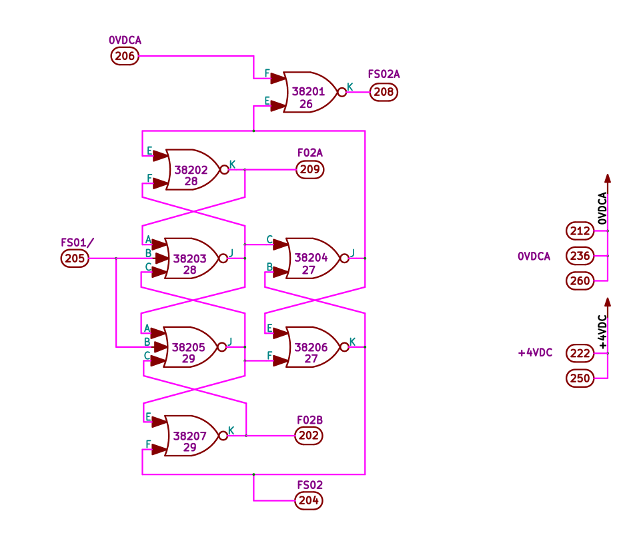
To simplify things, the testVerilog example cuts this all down so
that just the first of the many divide-by-two circuit
blocks. The abridged circuit produces the output signal FS02
from input signal FS01/ and implements what's known to electrical
engineers as a "flip-flop". Here is an image of that
circuit:
Workflow Step 2: One way to create the netlist is to load
the schematic file into eeschema, then from the main menu
select File/Export/Netlist/OrcadPCB2/ExportNetlist and create a
file called module.net. For this discussion, I did this
using KiCad v6, and got the resulting file
Workflow Step #3: Conversion to Verilog source code.
( { EESchema Netlist Version 1.1 created  Tue 14 Jan 2025 05:51:55 AM CST }
 ( /00000000-0000-0000-0000-00005d281baf $noname  J2 ConnectorA1-200
  (  202 Net-(J2-Pad202) )
  (  204 Net-(J2-Pad204) )
  (  205 Net-(J2-Pad205) )
  (  206 Net-(J2-Pad206) )
  (  208 Net-(J2-Pad208) )
  (  209 Net-(J2-Pad209) )
  (  212 0VDCA )
  (  222 +4VDC )
  (  236 0VDCA )
  (  250 +4VDC )
  (  260 0VDCA )
 )
 ( /00000000-0000-0000-0000-00005d281ba1 $noname  U129 D3NOR-+4VDC-0VDCA-ABC-E_F
  (    1 Net-(U127-Pad8) )
  (    2 Net-(J2-Pad202) )
  (    3 Net-(J2-Pad205) )
  (    4 Net-(U127-Pad2) )
  (    5 0VDCA )
  (    6 0VDCA )
  (    7 Net-(U127-Pad8) )
  (    8 Net-(J2-Pad204) )
  (    9 Net-(J2-Pad202) )
  (   10 +4VDC )
 )
 ( /00000000-0000-0000-0000-00005d281b3e $noname  U126 D3NOR-+4VDC-0VDCA-A_B-E_F
  (    6 0VDCA )
  (    7 Net-(U126-Pad7) )
  (    8 Net-(J2-Pad206) )
  (    9 Net-(J2-Pad208) )
 )
 ( /00000000-0000-0000-0000-00005d281b94 $noname  U127 D3NOR-+4VDC-0VDCA-B_C-E_F
  (    1 Net-(U126-Pad7) )
  (    2 Net-(U127-Pad2) )
  (    3 Net-(J2-Pad204) )
  (    4 0VDCA )
  (    5 0VDCA )
  (    6 0VDCA )
  (    7 Net-(U126-Pad7) )
  (    8 Net-(U127-Pad8) )
  (    9 Net-(J2-Pad204) )
  (   10 +4VDC )
 )
 ( /00000000-0000-0000-0000-00005d281b45 $noname  U128 D3NOR-+4VDC-0VDCA-ABC-E_F
  (    1 Net-(U127-Pad2) )
  (    2 Net-(U127-Pad8) )
  (    3 Net-(J2-Pad205) )
  (    4 Net-(J2-Pad209) )
  (    5 0VDCA )
  (    6 0VDCA )
  (    7 Net-(U126-Pad7) )
  (    8 Net-(U127-Pad2) )
  (    9 Net-(J2-Pad209) )
  (   10 +4VDC )
 )
)
*
dumbVerilog.py A1 module.net pins.txt 20 ../empty.init module.kicad_sch >module.vIn Windows, it would instead be
dumbInitialization0.py <module.v
dumbVerilog.py A1 module.net pins.txt 20 A1.init module.kicad_sch >module.v
python -m dumbVerilog A1 module.net pins.txt 20 ..\empty.init module.kicad_sch >module.vWhile in Mac OS, it would be
python -m dumbInitialization0 <module.v
python -m dumbVerilog A1 module.net pins.txt 20 A1.init module.kicad_sch >module.v
python3 -m dumbVerilog A1 module.net pins.txt 20 ..\empty.init module.kicad_sch >module.vThe details of this procedure are covered in the technical Appendix. In brief, pins.txt is a file describing backplane connections that are appropriate for AGC models 2003200 or 2003993, though it doesn't really serve any purpose here since the backplane is used only to interconnect multiple logic modules, whereas this circuit uses only a portion of a single logic module and thus doesn't connect to any other logic modules. 20 is the propagation delay of the NOR gates in nanoseconds. As I mentioned before, in this example circuit the various NOR gates form a flip-flop. The file A1.init is used to specify whether the flip-flop is initially "on" or "off" at the start of the digital simulation. It is a file that you can create manually — though generally with considerable inconvenience —, and the purpose of the first two steps of the process above is to heuristically create a version of A1.init that will probably be "good enough". In point of fact, the repository supplies a module.init for you that could have been used in place of A1.init in the third step above, so that the first two steps above could have been skipped. The A1.init generated above might look like
python3 -m dumbInitialization0 <module.v
python3 -m dumbVerilog A1 module.net pins.txt 20 A1.init module.kicad_sch >module.v
and is telling us that initially, we can choose output signal U127-J to be HIGH (1), U127-K to be LOW (0), U129-J to be HIGH, and U129-K to be LOW. I say it "might" look like that, because there are other consistent initial conditions that could be generated instead, such as:# Auto-generated for module A1 by dumbInitialization0.py.
U127 1 0
U129 1 0
The Verilog source code (module.v) that you get after the final step is below, depending on which initial conditions were generated. Even if you don't know Verilog, I think you can get some sense of what's what. The bulk of the file, namely theU126 0 1
U127 0 1
U128 1 0
assign statements, define how
the internal signals and output signals change at each timestep of
the simulation. The rst
signal is not present in the schematic, and is simply always added
by dumbVerilog.py. It's what allows the initial
conditions of memory — in this case, the flip-flop — to be set up,
but is normally active only at the very beginning of the
simulation. Verilog doesn't allow signal names like "FS01/",
because the character "/" isn't legal for signal names, so the
translator has automatically changed "FS01/" to "FS01_".Workflow Step #4: Creation of a test bench. This is the point in a simulation workflow where you would have to decide how you want the input signals supplied to the circuit to vary over time, as well as which output signals from the circuit you want to log for later viewing or analysis. Those decisions together comprise what's called the "test bench". The test bench could be yet another Verilog source-code file, though it turns out to be more-convenient for it to be a pair of files, one to hold your personal choices, and another to include anything that can be figured out via automation.// Verilog module auto-generated for AGC module A1 by dumbVerilog.py
module A1 (
rst, FS01_, F02A, F02B, FS02, FS02A
);
input wire rst, FS01_;
output wire F02A, F02B, FS02, FS02A;
parameter GATE_DELAY = 20; // This default may be overridden at compile time.
initial $display("Gate delay (A1) will be %f ns.", GATE_DELAY);
// Gate A1-U129A
pullup(g38205);
assign #GATE_DELAY g38205 = rst ? 1'bz : ((0|g38203|FS01_|F02B) ? 1'b0 : 1'bz);
// Gate A1-U129B
pullup(F02B);
assign #GATE_DELAY F02B = rst ? 0 : ((0|g38205|FS02) ? 1'b0 : 1'bz);
// Gate A1-U126B
pullup(FS02A);
assign #GATE_DELAY FS02A = rst ? 0 : ((0|g38204) ? 1'b0 : 1'bz);
// Gate A1-U127A
pullup(g38204);
assign #GATE_DELAY g38204 = rst ? 1'bz : ((0|FS02|g38203) ? 1'b0 : 1'bz);
// Gate A1-U127B
pullup(FS02);
assign #GATE_DELAY FS02 = rst ? 0 : ((0|g38204|g38205) ? 1'b0 : 1'bz);
// Gate A1-U128A
pullup(g38203);
assign #GATE_DELAY g38203 = rst ? 0 : ((0|F02A|FS01_|g38205) ? 1'b0 : 1'bz);
// Gate A1-U128B
pullup(F02A);
assign #GATE_DELAY F02A = rst ? 0 : ((0|g38204|g38203) ? 1'b0 : 1'bz);
// End of NOR gates
endmodule
which gives you the following:# In Linux:
dumbTestbench.py <module.v >module_tb.v
# Or in Windows:
python -m dumbTestbench <module.v >module_tb.v
# Or in Mac OS:
python3 -m dumbTestbench <module.v >module_tb.v
You needn't worry (I hope!) about what any of that means. I'll just point out that it tells the emulator that the basic time scale of the simulation is 1 nanosecond (with a precision of 1 picosecond), the propagation delay through the NOR gates is by default 20 nanoseconds, and that the file tb.v, which is where the "personal choices" mentioned above are stored, is automatically imported.// Verilog testbench created by dumbTestbench.py
`timescale 1ns / 1ps
module agc;
parameter GATE_DELAY = 20;
`include "tb.v"
wire F02A, F02B, FS02, FS02A;
A1 iA1 (
rst, FS01_, F02A, F02B, FS02, FS02A
);
defparam iA1.GATE_DELAY = GATE_DELAY;
endmodule
The "// Include-file used by module_tb.py for automating testbench generation.
reg rst = 1;
initial begin
// Assumes compilation with the -fst option.
$dumpfile("module.fst");
$dumpvars(0, agc);
# 2000 rst = 0;
# 500000 $finish;
end
reg FS01_ = 0;
always #9765.625 FS01_ = !FS01_;
initial
$timeformat(-6, 0, " us", 10);
initial
$monitor("At time %t, rst=%d, FS01_=%d, F02B=%d, FS02=%d, FS02A=%d, FS02A=%d", $time, rst, FS01_, F02B, FS02, F02A, FS02A);
reg rst = 1" means
that the rst signal is
going to be an input signal into the circuit we're testing, but here
within the test bench it's going to be a "register" that remembers
it's own settings, as opposed to a "wire" (which cannot remember
anything). Thus, we set rst
to 1 and it will stay that way until we say otherwise. A few
lines later we will see "# 2000 rst = 0",
which means that 2000 nanoseconds (2 μs) after startup, the test
bench is going to reset the rst
signal to 0, and leave it there. The "#
500000 $finish" that you will also see there says
that the simulation itself will actually end after 500 μs. The
intervening "$dumpfile"
and "$dumpvars" statements
say that an output log-file called testVerilog.fst is going to be
opened, and that the values of all of the input and output variables
are going to be dumped into it on a cycle-by-cycle basis, for later
analysis. reg FS01_ = 0" means
that FS01_ (FS01/) is
also an input to the circuit being tested, and that it starts out at
0. But "always #9765.625 FS01_ =
!FS01_" means that FS01_
is going to be toggled every 9.765625 μs during the
simulation. Recall that FS01/ is a 51.2 KHz square wave in the
AGC, and therefore it toggles from low-to-high or high-to-low at a
rate of 102.4 KHz, or (surprise!) every 9.765625 μs.initial"
statements at the very end describe the status messages which the
simulation is going to print out whilst running. These
messages are just informative, and have nothing to do with the data
being dumped out on the module.fst. You don't even need to
print out any status messages if you don't want to.I can't show you the contents of module.vvp — I bet you're relieved! —, since it's a binary file rather than a human-readable one.iverilog -o module.vvp module_tb.v module.v
I get messages something like this when I do that:vvp module.vvp -fst
Gate delay (A1) will be 20.000000 ns.Thus as promised,
FST info: dumpfile module.fst opened for output.
At time 0 us, rst=1, FS01_=0, F02B=x, FS02=x, FS02A=x, FS02A=x
At time 0 us, rst=1, FS01_=0, F02B=0, FS02=0, FS02A=0, FS02A=0
At time 2 us, rst=0, FS01_=0, F02B=0, FS02=0, FS02A=0, FS02A=0
At time 9 us, rst=0, FS01_=1, F02B=0, FS02=0, FS02A=0, FS02A=0
At time 9 us, rst=0, FS01_=1, F02B=1, FS02=0, FS02A=0, FS02A=0
At time 19 us, rst=0, FS01_=0, F02B=1, FS02=0, FS02A=0, FS02A=0
At time 19 us, rst=0, FS01_=0, F02B=1, FS02=1, FS02A=0, FS02A=1
At time 19 us, rst=0, FS01_=0, F02B=0, FS02=1, FS02A=0, FS02A=1
At time 29 us, rst=0, FS01_=1, F02B=0, FS02=1, FS02A=0, FS02A=1
At time 29 us, rst=0, FS01_=1, F02B=0, FS02=1, FS02A=1, FS02A=1
At time 39 us, rst=0, FS01_=0, F02B=0, FS02=1, FS02A=1, FS02A=1
At time 39 us, rst=0, FS01_=0, F02B=0, FS02=0, FS02A=1, FS02A=1
At time 39 us, rst=0, FS01_=0, F02B=0, FS02=0, FS02A=0, FS02A=0
At time 48 us, rst=0, FS01_=1, F02B=0, FS02=0, FS02A=0, FS02A=0
At time 48 us, rst=0, FS01_=1, F02B=1, FS02=0, FS02A=0, FS02A=0
...
At time 468 us, rst=0, FS01_=0, F02B=0, FS02=0, FS02A=0, FS02A=0
At time 478 us, rst=0, FS01_=1, F02B=0, FS02=0, FS02A=0, FS02A=0
At time 478 us, rst=0, FS01_=1, F02B=1, FS02=0, FS02A=0, FS02A=0
At time 488 us, rst=0, FS01_=0, F02B=1, FS02=0, FS02A=0, FS02A=0
At time 488 us, rst=0, FS01_=0, F02B=1, FS02=1, FS02A=0, FS02A=1
At time 488 us, rst=0, FS01_=0, F02B=0, FS02=1, FS02A=0, FS02A=1
At time 498 us, rst=0, FS01_=1, F02B=0, FS02=1, FS02A=0, FS02A=1
At time 498 us, rst=0, FS01_=1, F02B=0, FS02=1, FS02A=1, FS02A=1
FS01_
(FS01/) toggles about every 10 microseconds, while FS02 toggles about every 20
microseconds, though it's a bit of a pain to extract that conclusion
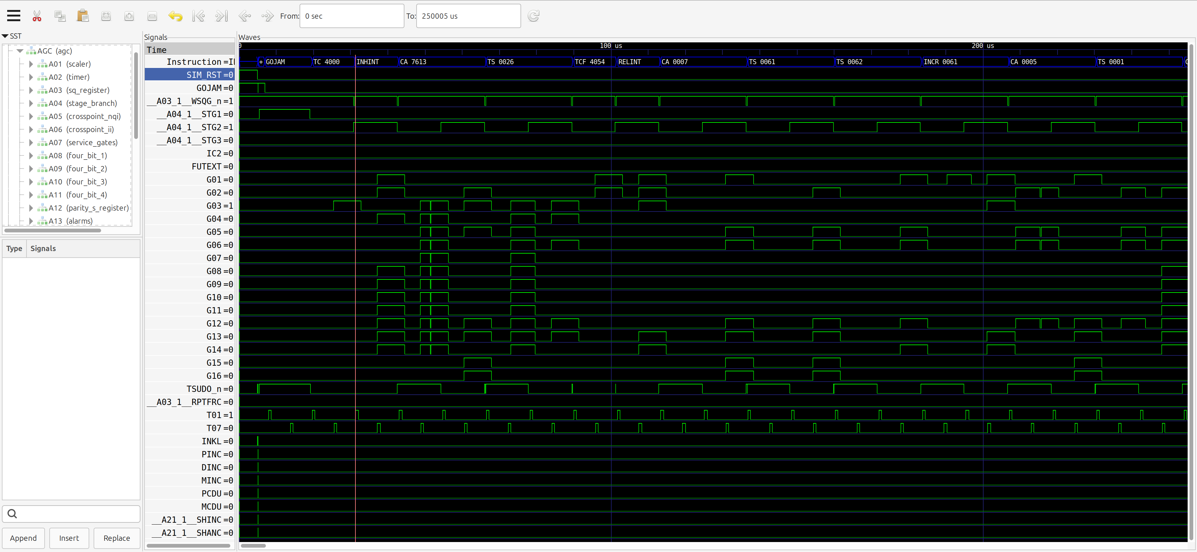
from the messages.Workflow Step #8: Visualization. Pull the dump-file created by running the simulation, namely module.fst, into the GTKWave visualization program,
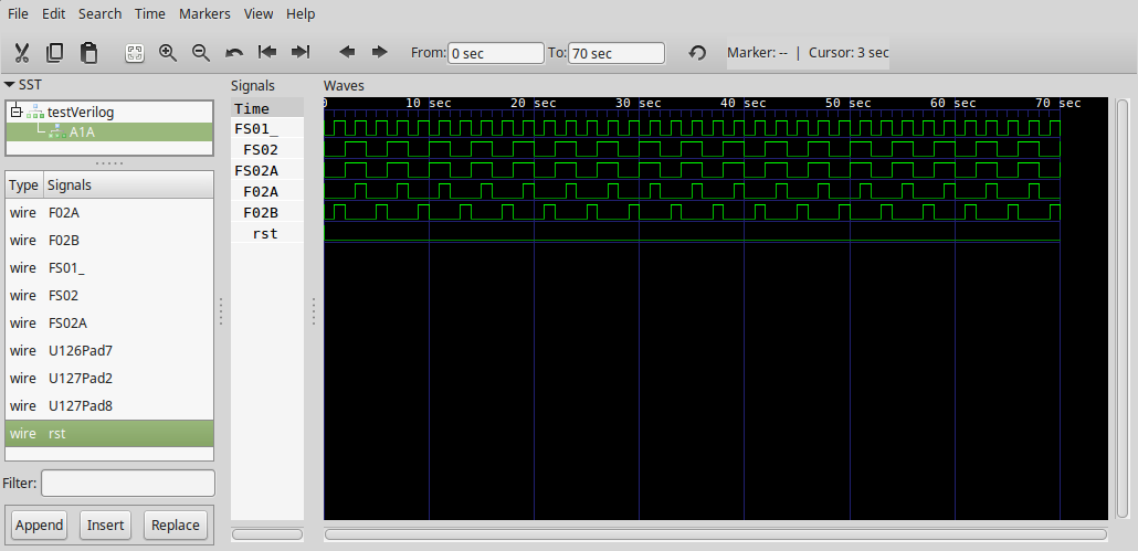
In Mac OS, I think it would just be easier to open GTKWave from the desktop (rather than figuring out how to do it from a command line), and use its File menu to navigate to virtualagc-schematics/Schematics/testVerilog/module.fst.# In Linux or Windows:
gtkwave module.fst
Aside: Actually, I won't pretend that what you see will magically resemble the screenshot. There will a few interactive steps within the GTKWave program's user interface to set the viewing timescale, select the specific signals to view, and the order in which the signals should appear, but I don't want to get sidetracked into a discussion of GTKWave's operation. If you've been motivated enough to get this far, I think you can figure those bits out for yourself! But you can look at GTKwave's online documentation to see how to use the visualizer, if you cannot monkey through it yourself. Or you can try these steps to quickly get something reasonably viewable, even it won't look precisely like the screenshot:
- Select some signals to view:
- Left-Click on where it says "agc" in the SST pane. That will open up a subheading called "iA1 (A1)".
- Right-Click on the subheading "iA1 (A1)" in the SST pane.
- In the pop-up menu that appears, choose Recurse-Import / Append / Yes.
- Zoom out a bit by clicking the Zoom-Fit hot-button in the toolbar at the top. (In the screenshot below, that's the button between the clipboard button and the + button.)

Note: While the waveforms shown in the two graphs are the same, there is nevertheless a significant difference: Figure 4-121 purports to display the signal FS01, whereas our data visualization displays signal FS01/, which is inverted from FS01. Then too, the position of the final pulse of F02B doesn't match. One of us must be wrong! Which one could it be? Could it be ... me? Could it be ... them? The suspense is terrible! I hope it'll last. Check it out yourself.
Cheat sheet: I've made most of this line white-on-white, to make it harder to read accidentally. If you highlight this entire line, I expect it will be enlightening. To figure out who's wrong, it's relatively easy to work backward from the condition F02A HIGH to see what conditions it requires for the inputs of the various NOR gates, then to work backward to the NOR gates feeding those inputs, and so on. You'll quickly find that F02A HIGH implies that FS01/ is HIGH as well, which means that Figure 4-121 is wrong in asserting that F02A is HIGH at the same time as FS01 is HIGH. Identical reasoning applies to determining the conditions for F02B being HIGH, demonstrating that Figure 4-121 is incorrect about the positioning of the final pulse.
| Generic AGC Model |
Block |
Mission |
Spacecraft |
Specific Dash Number |
|---|---|---|---|---|
| 1003565 |
I |
AS-202 |
CM |
1003565-011 |
| 1003700 |
I |
Apollo 4 |
CM |
1003700-051 |
| Apollo 6 |
CM |
1003700-071 |
||
| 2003100 |
II |
2TV-1 |
CM |
2003100-061 |
| II |
LTA-8 |
LM |
2003100-071 |
|
| 2003200 |
II |
(None) |
CM |
2003200-031 |
| (None) |
LM |
2003200-041 |
||
| 2003993 |
II |
Apollo 5 |
LM |
2003993-011 |
| Apollo 7 | CM | 2003993-031 | ||
| etc. |
||||
Aside: Model 2003993, in differing specific dash numbers, was used for almost all missions, so I hope you'll forgive me for running out of steam at the end of the table and just covering all of the remaining missions with a bland "etc." rather than giving you 20+ more rows of model 2003993! The way to get the information for the missing entries is by drilling down into the GN&C mission hierarchy table. That is also the place to go in order to match a particular AGC model to a specific set of electrical schematics.
But there are really less choices than it appears at first
glance. There's a table in the Technical Appendix that lists all
of the logic modules appearing in the different AGC models, in
terms of the assocated schematic-diagram drawing numbers, and we
can summarize what we learn from that table as follows:
Or in other words, the only essentially-different cases that we
could potentially simulate are AGC model 1003700 (Block I) or
model 2003993 (Block II).
Regarding the choice of AGC software: In principle, any of the available Block I AGC software versions can be used in a simulated AGC model 1003700, while any of the available Block II AGC software versions can be used in a simulated AGC model 2003993. Any Block II core-rope — in the form of a "bin" file produced by the AGC assembler, yaYUL — can be converted to a Verilog source code by a Python program provided by Mike Stewart that's called bin_to_verilog_rom.py. In practice, 15 or so AGC software versions have been converted by Mike and are already found with the transcribed schematics, in a folder called "roms". I would recommend the program called "Validation-hardware-simulation".Aside: And of those two choices, only the simulation workflow for Block II has been debugged so far and can be considered mature enough to be "working" ... which coincidentally, is the one that is likely most desired by people, since it's the one relevant to Apollo 11.
Regarding the test bench: This is really no different than
what was discussed in the preceding section, except that we need a
test bench for the entire AGC, rather than test benches for
individual logic modules. I have created some test-bench
files that can be used as starting points. They are named
tb-2003993.v, tb-2003200.v, etc. Some of the characteristics
of the test bench (such as the run length and the selection of
logged signals) can be changed at runtime rather than requiring
modifications to these test-bench source-code files themselves; see the Technical
Appendix.
Aside: As in the case of simulating a single module, I've provided a script (simulateAGC for Linux/Mac or simulateAGC.bat for Windows) which can perform the entire sequence of steps needed to carry out the simulation, assuming that the choices described in the preceding section have been made. The script is run from the Schematics directory, and its calling sequence from the command line isWhat makes whole-AGC simulations trickier than single module simulations is that while the same basic workflow holds, some of the steps of the workflow are carried out for each logic module comprising the circuit, while other steps combine the logic-module-specific files into single large files pertaining to the whole AGC, and yet other steps operate on those whole-AGC files.
wheresimulateAGC AGC_MODEL SOFTWARE VERILOG_OPTIONSAGC_MODELdefaults to "2003993",SOFTWAREdefaults to "Validation-hardware-simulation", andVERILOG_OPTIONS(a quoted list of command-line parameters for the Verilog compiler that alter values in the test bench) is empty (""). The settings you can include inVERILOG_OPTIONSare described in the Technical Appendix.
To run the simulation while accepting all of the defaults, you could use the simple command.
This will perform the entire workflow for 0.25 seconds of simulated time and thus jump you right to the visualization of the data output by the simulation, thus avoiding the unpleasant possibility of having to learn anything in the meantime. Among the useful files left behind are the simulation file AGC_MODEL.vvp (in case you'd like to re-run the simulation), and agc.fst (the results of the simulation run, in case you'd like to re-view them at some later time).simulateAGC
Aside: Note that the while the AGC's physical memory, both erasable and fixed, was binary in the sense that it stored 1's and 0's, it was not implemented by digital circuitry. Instead, it was analog circuitry that had the effect of flipping the magnetic fields of memory cores. As such, AGC memory schematics cannot be converted to Verilog source code, nor simulated by Verilog. At least, not if used as-ins. Instead, what has been done is that the memory has been modeled by digital circuits having the same inputs and outputs as the original AGC circuitry, but differing completely internally. Moreover, unlike all other AGC digital circuitry, the memory model is not implemented using triple-input NOR gates, but is instead implemented by more modern RAM, ROM, and other chips, which are themselves modeled by pure Verilog source code. See the schematic diagram and associated Verilog source code in Schematics/fixed_erasable_memory/. I did not develop this modeling of the AGC memory; rather, Mike Stewart had already developed it for his own AGC electrical simulation, as mentioned earlier, and it has simply been appropriated for use in the Virtual AGC electrical-simulation framework. Thanks again, Mike!Four separate things go into simulation of erasable and fixed memory:
Combining those ideas, what Step #5 of the workflow does is to
copy the appropriate file Schematics/roms/SOFTWARE_VERSION.v
to Schematics/roms/rom.v. Since RAM.v, ROM.v, and BUFFER.v
already exist and are never changed, nothing needs to be done with
them.
Workflow Step #6 (compilation of the Verilog). The compiler, iverilog,
uses all of the Verilog source-code files as inputs —
specifically, AGC_MODEL_tb.v, module.v for each of
the AGC's logic modules, RAM.v, ROM.v, rom.v, and BUFFER.v
—, to create the simulation itself, which will be a file
called AGC_MODEL.vvp.
Aside: Don't worry about the notion that we have different Verilog source-code files called ROM.v and rom.v that might be confused with each other because of the loony notion in Mac OS and Windows that filenames could be case-insensitive. Those source-code files are in different folders, so even Mac OS and Windows can't get them mixed up.
Workflow Step #7 (performing the simulation):
This creates a simulation-result "dump file" called agc.fst, in which the signals selected by the test bench are logged for subsequent viewing or analysis.vvp AGC_MODEL.vvp -fst
whereas in Windows,gtkwave agc.gtkw
You'll notice that this command is somewhat different than what we saw in the simulation of an individual module, from which we would have instead suspected a command of "gtkwave agc-windows.gtkw
gtkwave


        agc.fst
". Make no mistake: the latter
command would have worked fine! But unlike the case of a
single-module simulation, in the case of a full-AGC simulation we
are actually in a position to make a guess as to which signal-traces
might be usefully displayed. And as we'll see in the next
section, there are certain enhancements that can be made to our
signal-viewing experience when an entire AGC is being
analyzed. You can think of the provided agc.gtkw and
agc-windows.gtkw files, or a similar ones, as representatives of a
kind of "project-settings" file that helps us to apply those
improvements to the viewing experience without having to manually
perform a lot of tedious interactive setup within the GTKWave
user interface.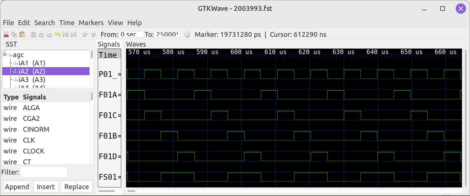

There! That neatly explains, I think, why I'm right, and
everyone else is to blame for any apparent errors, and how my
simulation is beautiful and perfect. And they said it could
not be done! My next trick will to be to run for public
office of some kind. On the other hand, alternative
explanations concluding that I and my simulations are idiotic are
welcome too. Well, perhaps not welcome exactly
.... but I say, anything that advances the dialog! Let
me know if you come up with one.
GTKWave's contribution is a feature in which you can
optionally apply a so-called "transaction
filter" to a selection of signals. A transaction
filter is a user-supplied program, in our case written in Python
3, that is applied by GTKWave at each change to the
levels of any of the selected signals. The transaction
filter can then process the levels of the selected signals in any
manner it chooses, and can do things like log the results of its
calculations to a file or add a new trace containing those results
to GTKWave's display of the signals.
One of Mike's contributions, among many others, is to actually
supply such a transaction filter that decodes the AGC signals as
CPU instructions, displaying the resulting instructions and their
operands as an additional trace. I briefly mentioned in the References section
earlier that Mike had performed his own functionally-equivalent
transcription into KiCad of the AGC electronics, along
with the associated simulations thereof. Although I provide
no instructions for doing so here, just as you can run the Virtual
AGC simulations based on the Virtual AGC transcriptions of the AGC
electrical schematics, if you refer to Mike's website you could
alternatively use Mike's transcriptions of the AGC electrical
schematics and run simulations based on them.
Aside: Since I seem to be implying that Mike's simulations are so terrific — which I am — you may wonder why in the world you would choose to use Virtual AGC schematics and simulations rather than Mike's. The question is a valid one. The answer is that it's a matter of personal preference. Here's a rough point-by-point comparison:
Mike Stewart
Virtual AGC
Schematics are functionally equivalent to Apollo
Schematics are visually identical to Apollo drawings
Requires modified version of KiCad
Uses stock version of KiCad
Simulations run faster
Simulations run slower
Hard to compare to Apollo drawings
Easy to verify vs Apollo drawings
Documentation is in Mike's GitHub repository
Documentation is the stuff you've been reading
Did it all first
Copycat, piggybacking in some ways on Mike's work
Below (click to enlarge!), you can see a
screenshot from one of Mike's simulations, with the
instruction-decoder transaction filter displaying the AGC
instructions along the top:
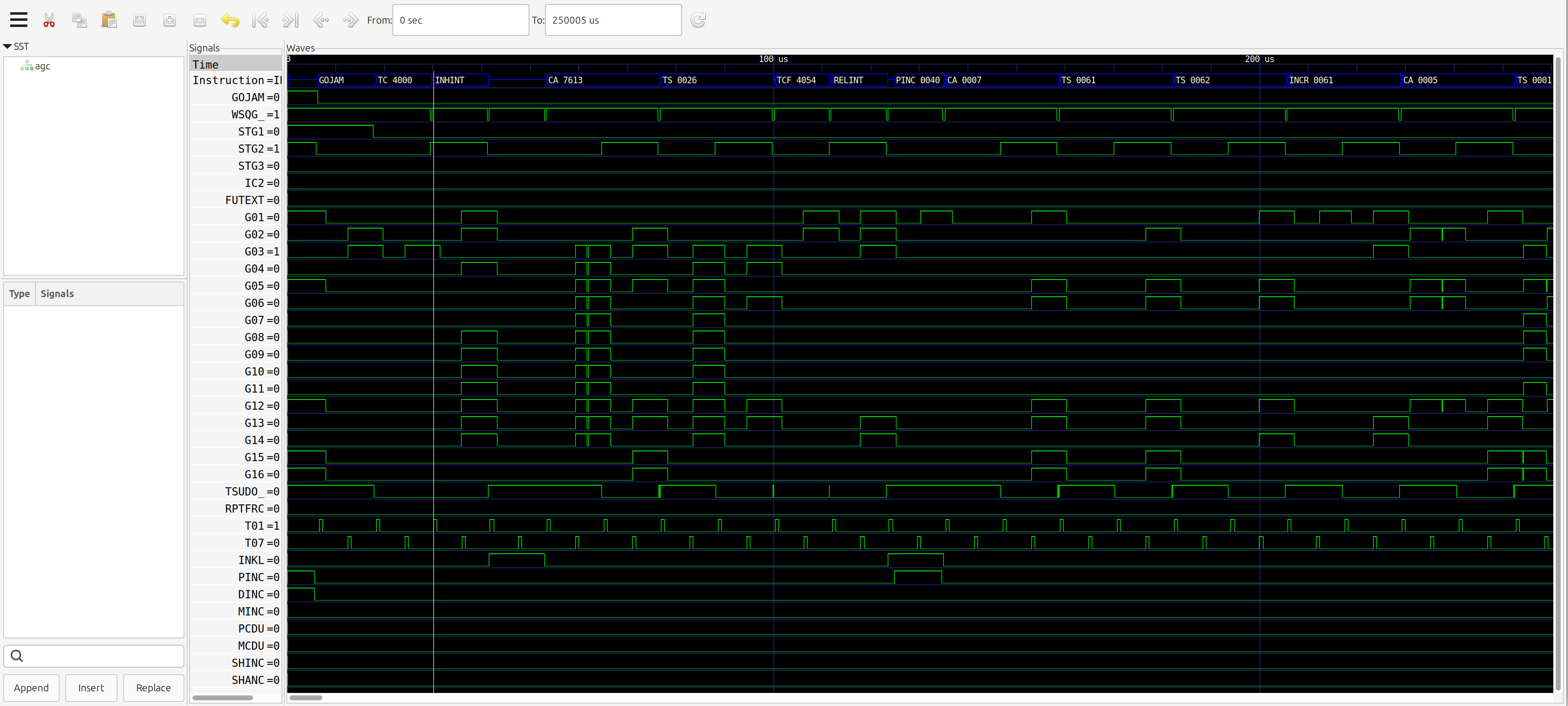
| Mike's Simulation |
Virtual AGC Simulation |
|---|---|
GOJAM |
|
Aside: Or in other words, if you were to perform exactly the same simulation as I did above, following precisely the same steps, you might get a slightly-different result because I could have improved (or at least changed) the algorithm performing the flip-flop initializations in the meantime. Remember that in the physical AGC, there's little effort to perform any such initialization except in a few crucial cases, and the expectation was that after power-up the flip-flops would just settle on their own into some benign mutually-consistent configuration. So it's hard to be too terribly worried that we're treating initialization of the flip-flops somewhat loosely ourselves.As for whether the particular AGC instructions being executed make sense, recall that while you can in principle simulate the AGC CPU running any AGC software, by default the AGC program used is the one called "Validation-hardware-simulation". Like all AGC programs, execution begins at address octal 4000 after a GOJAM, so the initial TC 4000 reported by the transaction filter is in fact an instruction manufactured entirely by the CPU hardware, rather than being something explicit in the AGC program's source code. In other words, a GOJAM always immediately triggers a TC 4000. The assembly listing of the source code looks like this:
In point of fact, I was comparing apples-to-oranges anyway, since Mike's simulation was of AGC model 2003993 and mine was of model 2003200, and used a preliminary version of the simulation framework to boot! If you were to run a new simulation today, of a 2003993, you'd actually find it very difficult to discern any difference from Mike's simulation, except in the first few microseconds when the AGC is settling down. But I keep the older screenshot here because it's more pedagogically useful to be able to explain the discrepancies than to lack any discrepancies to explain!
Using a little imagination, and some judicious color-coding, you can see that exactly the instructions we expect are being executed by both of the simulations. Bear in mind that the symbol ZEROES refers to CPU register 0007 (which is always filled with zeroes) rather than to a variable, and similarly CPU register 0005 is the Z register, CPU register 0001 is the L register, CPU register 0026 is the TIME3 register, and so on.000061,000061: 4000 00004 INHINT # GO
000062,000062: 4001 37613 CA O37774 # Schedule the first TIME3 interrupt
000063,000063: 4002 54026 TS TIME3 #
000064,000064: 4003 14054 TCF INIT # Proceed with initialization
000121,000121: 4054 00003 INIT RELINT #
000122,000122: 4055 30007 CA ZEROES # zero out A
000123,000123: 4056 54061 TS ERRNUM # and the error-code
000124,000124: 4057 54062 TS ERRSUB #
... Some comments omitted ...
000152,000152: 4060 24061 INCR ERRNUM #
000153,000153: 4061 30005 CA Z # fetch Z.
000154,000154: 4062 54001 DEST1 TS L #
.
.
.
Unmodified AGC software may not be 100% suitable for the purposes
of digitally simulating the AGC electronics, and may require some
modifications in order to be suitable. At this writing, the
only example of this is in the Validation
program, which is a small suite of test routines for the AGC CPU
that I wrote, based on the original documentation. However,
Validation is an interactive program, and dependence on a DSKY may
not be very desirable in the context of simulating the digital
electronics of the AGC. Much better to run AGC software
which doesn't have to wait for the (non-existent) astronaut to do
something on the (non-existent) DSKY! One approach to this
problem would be simply to clone the AGC program one wishes to
run, and then make whatever changes were desired directly to the
cloned source code.
Another approach is to embed directives in the original AGC
program that act like conditional compilation, so that sections of
the source code can be modified at assembly time without
maintaining two copies of the source code. The assembler (yaYUL)
supports this approach via a command-line switch, --simulation, and embedded
directives -SIMULATION
or +SIMULATION within end-of-line
comments in the AGC source code. Lines of AGC source
code without either of these embedded directives, or with those
directives embedded in full-line comments, are processed normally
by yaYUL whether or not the --simulation
command-line switch is present. However, if --simulation is in effect, yaYUL
comments out any lines with an embedded -SIMULATION
directive. Conversely, if --simulation
is not in effect, yaYUL comments out any lines
with an embedded +SIMULATION
directive.
The AGC Validation program has such directives embedded in it,
and when assembled with --simulation
produces a version of the program more-suitable for simulating the
AGC electronics. This alternate version of Validation is
known as Validation-hardware-simulation, and thus is the program
run by default when simulating the AGC electronics.
More-sophisticated AGC test programs (such as Borealis) and the
original test programs (like Aurora and Sundial) are available as
well, but they have not received the treatment mentioned above, as
of this writing.
This is too detailed a topic for me to give much helpful advice
about in a limited space. Plus, I consider it unlikely that
you'll find yourself needing to transcribe an AGC-related
schematic diagram. I will simply point out the following:
There are two methods.
Method 1: While viewing the top-level page of a schematic
diagram in eeschema, select File/Export/Netlist from the
main menu. In the "Export Netlist" window which pops up,
select the tab labeled "OrcadPCB2" and click the button labeled
"Export Netlist". In the "Save Netlist File" dialog which
appears, which should have pre-chosen the folder containing the
top-level schematic file itself, save the netlist as "module.net".
Method 2: For KiCad v.7 or later, the netlist can be
created from a command line without even running eeschema.
The command would be
kicad-cli sch export netlist --output module.net --format orcadpcb2 module.kicad_sch
Aside: To be completely honest, I'm no longer entirely sure how many of these rules the supplied tools actually depend upon, as opposed to these rules just being the ones obeyed by the original developers. Most of them are relied upon.To convert a single schematic to Verilog source code, the Python 3 script dumbVerilog.py is used:
dumbVerilog.py MODULE module.net pins.txt DELAY module.init module.kicad_sch [WIRETYPE] >module.vThe files called pins.txt and module.init are covered in the succeeding sections. The file pins.txt will be searched for if not found; it may be either in the current directory, the directory containing dumbVerilog.py itself (the usual case), or else specified with an explicit path. The parameters "module.net", "module.kicad_sch" (or just "module.sch" for KiCad v.5), and "module.v" are generally literal. As for the remaining command-line parameters:
MODULE would be something like "A1", "A2",
etc. It's the designation of the specific logic module to
which the schematic belongs. The tool doesn't actually use
this for anything except as a unique identifier when multiple
logic modules are interconnected, so if you're working with a
circuit other than the official AGC modules, it doesn't really
matter what you use here, though I would recommend that it still
be of the form Ann.DELAY, roughly speaking, is the
propagation delay of signals from the input of a NOR gate to its
output. The unit in which DELAY is
expressed ultimately depends upon the time-scale that will be
set in the test bench, but that's conventionally 100 ns.
The nominal gate delay of AGC NOR gates was 20 ns, so that means
a reasonable DELAY might be 0.2.WIRETYPE is an optional parameter having
the value either "wire" or "wand".
It shouldn't matter which is chosen, so this parameter should
probably be omitted.Abstractly, the AGC circuitry consists of a number of "modules"
(each represented by an electrical schematic), plugged into a
"backplane". The backplane, again abstractly, consists of a
set of connectors whose pins are interconnected by wires.
However, there is no schematic diagram as such for the backplane,
so to incorporate the backplane into our simulation the
interconnections in the backplane must be specified in some other
form. That alternate form of description is the pins.txt
file, which is just a text file having a separate line in it for
each pin of each connector on the backplane.
Each line of the file has four fields, delimited by space
characters. Those fields are:
Aside: Technically, there are actually two separate backplanes, designated "A" and "B", into which the AGC modules Ann and Bnn respectively plug, with some interconnections between the two backplanes. The pins.txt file describes both, so we may as well think of it simply as one big backplane.
Regarding the module-to-backplane connectors, for the logic
modules that interest us for simulation purposes, each module had
a physical 284-pin connector consisting of 4 rows of 71 pins
each. (The 21st pin from either end of a row was missing, so
you could equally-well consider it physically to be a 276-pin
connector consisting of 4 rows of 69 pins each. But the pin
numbering pretends that the missing pins were present.) On
the other hand, on the electrical schematics for the logic
modules, each of the 71-pin rows was considered a separate
connector, and thus the schematics show 4 separate connectors
each, designated as J1, J2, J3, and J4.
Just to emphasize this point, in case the message was lost in the
details: In pins.txt each backplane connector for a logic
module has 284 pins, while on the logic module's electrical
schematics there are instead 4 connectors of 71 pins each.
In principle, a separate pins.txt file should be used for each
different AGC model. In practice, there's little difference
between AGC models 2003200 and 2003993, and so there is presently
a single pins.txt file used for those two models. As far as
other AGC models is concerned, there is presently no available
pins.txt for them.
Aside: Strictly speaking, this isn't quite true. The existing pins.txt was derived from Mike Stewart's digital simulation of the AGC. Mike's backplane pin data was derived in turn by a script that analyzed his Verilog files. Thus if we indeed wanted to generate a separate pins.txt file for each Block II AGC model we'd have an awkward chicken-and-egg problem, since dumbVerilog.py needs pins.txt before generating our Verilog files, whereas the only automated way of generating pins.txt does so after creating the Verilog files. On the other hand, for Block I AGC's I've created a similar file, pinsBlockI.txt, by processing Block I schematics (rather than Verilog files) using an AWK script, so perhaps the same technique could be used for Block II as well. However, the pinsBlockI.txt file is in a somewhat different format than pins.txt, and dumbVerilog.py isn't presently able to support that particular format. Although I don't recall for certain, I suppose this means that I had only done preliminary work on Block I AGC simulation, without having taken it to the point of the simulation actually functioning.
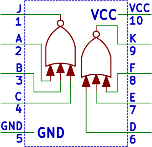 The only digital components
present in AGC logic-module schematics are dual triple-input
open-drain NOR gates (as in the figure to the left), which in
themselves are stateless; i.e., the output signal of a NOR gate is
directly determined by the current state of its input
signals. Or at least, the output is determined by the state
of the input signals after however long it takes the signals to
propagate through the gate, which is nominally 20
nanoseconds. Nevertheless, it is possible to interconnect
NOR gates in such a way that a block of NOR gates has an output
signal that does not necessarily depend on the current state of
the inputs. In other words, the block of NOR gates has
"memory". The most-common such circuit block in the AGC uses
several NOR gates to form what's known as a "flip-flop"; i.e., a
memory element capable of indefinitely storing a single bit
indefinitely. Or rather, of storing a bit until the power is
cycled, at which point the value of the bit is lost. The
testVerilog circuit used in examples above is such a
flip-flop.
The only digital components
present in AGC logic-module schematics are dual triple-input
open-drain NOR gates (as in the figure to the left), which in
themselves are stateless; i.e., the output signal of a NOR gate is
directly determined by the current state of its input
signals. Or at least, the output is determined by the state
of the input signals after however long it takes the signals to
propagate through the gate, which is nominally 20
nanoseconds. Nevertheless, it is possible to interconnect
NOR gates in such a way that a block of NOR gates has an output
signal that does not necessarily depend on the current state of
the inputs. In other words, the block of NOR gates has
"memory". The most-common such circuit block in the AGC uses
several NOR gates to form what's known as a "flip-flop"; i.e., a
memory element capable of indefinitely storing a single bit
indefinitely. Or rather, of storing a bit until the power is
cycled, at which point the value of the bit is lost. The
testVerilog circuit used in examples above is such a
flip-flop.
This has an implication on the initial conditions for a digital
simulation, since it might be useful to specify not only the
levels of the input signals to the circuit being simulated, but
the initial states of these implicit flip-flops as well. After
power-up the simulation itself takes care of computing their
states at later times. But the simulation first has to have
some way of knowing what the states were at power-up in order to
do that.
In the design of the physical AGC, almost no effort was
given to putting these implicit flip-flops into any given
state. (And in those cases where an effort had been made,
the mechanisms used would put the simulated flip-flops into a
known state too.) Rather, the developers just seemed to feel
that the flip-flops would generally settle down into some
stable state, and that happy thought proved to be adequate for
their purposes. For our purposes, namely digital
simulation, it's not enough! In simulation, it's
perfectly possible for a such a flip-flop to oscillate
indefinitely without ever settling down into some stable
state. Indeed, that has happened to me many times. Not
good!
One way to guarantee that the simulation will settle into a
stable state is to give it initial conditions in which it's already
in a stable state. Not all logical networks of NOR gates
have have such a stable state. If, for example, our circuit
consisted of a single NOR gate in which two of the inputs were
tied LOW but the third input was connected to the output, then
there is no logically-consistent set of signals, and the signal
values change with each timestep. But besides being stable,
we'd also like other properties to be satisfied, such as that all
counter registers are zeroed out and that the RAM isn't being
simultaneously read and written to. That the AGC does have
some stable states we do know, simply because we do know that it
can be simulated. Alas, finding such stable states with the
additional constraints we'd like to impose has proven
tricky. So in the interest of having a simulation which
settles down, we're generally forced to start with some state
having other properties that may not be entirely to our liking.
Aside: Why the difference between the physical AGC and the simulated AGC? Why does a physical AGC quickly settle into a logically-consistent set of signal values, while Verilog simulation of it does not necessarily do so? I think it probably has to do with the fact that in the Verilog simulation, all of the logic gates have the same propagation delay at all times, whereas in a physical AGC the gates are all little different, as well as having propagation delays that vary with temperature and somewhat over time. The result is that there's a certain random element present in the evaluation order of the logic gates in the physical AGC that's not present in the simulation. Besides which, in a physical AGC, the logic gates are still analog circuits, so a difference of (say) a tenth of a volt has some effect, while in the digital simulation they're purely digital (exact 1's and 0's).
To specify the initial states of flip-flops, module.init allows
you to state the initial output signal of any or all of the NOR
gates. As we say in the figure above, a dual NOR-gate
component used in the AGC has two outputs, which are designated as
pin J for one of the NOR gates and K for the other of the NOR
gates. The way these are specified in module.init is that
there is a line in the file for each dual NOR component that you
want to specify, and that line has the format
Unnn OutputJ [ OutputK [ DelayJ [ DelayK ] ] ]where Unnn is the reference designator of the dual-NOR component and OutputJ and OutputK are the output signal levels (0 or 1, default 0) at pins J and K of the dual-NOR component. DelayJ and DelayK are the respective propagation delays for the two NOR gates, in units as described for the DELAY parameter of dumbVerilog.py as discussed earlier, which is also the default for any omitted DelayJ or DelayK.
 You can also
annotate the module.init file with comments (preceded by "#") or
blank lines, if it helps you document what's being done.
You can also
annotate the module.init file with comments (preceded by "#") or
blank lines, if it helps you document what's being done.U127 1 0
U129 1 0
In other words, U127's J output is 1 ("on") and K output is 0
("off"); and the same for U129. I've illustrated that in the
image to the right by coloring NOR-gate outputs specified
initially as 1 in green, and those
specified initially as 0 in red.
You don't need to specify the output for every NOR gate, and thus
the outputs of U126 and U128 are left unspecified. But if
you manually create the module.init file, it's entirely up to you
to determine which ones you want to specify; and since not all
possible combinations of signals are logically consistent, you
must insure the consistency, which can be quite tiresome if done
manually. Because of the way NOR gates work, specifying that
U129's OutputJ is 1 forces U127 OutputK, U128 OutputJ, and
U129 OutputK all to be 0. So if you specified any of those
latter outputs to be 1, you'd be creating an inconsistent set of
inital conditions.
dumbInitialization.py <TheVerilogSourceCode.v
where TheVerilogSourceCode.v is
(surprise!) the Verilog source-code for which you wish to generate
some initialization information. There are actually two
basically-different scenarios in terms of acquiring the TheVerilogSourceCode.v
file:
Important note: There are actually two such Python scripts provided, dumbInitialization.py and dumbInitialization0.py, with identical calling sequences. The practical difference between them is that they use different algorithms, and therefore have different convergence, as well as very likely producing different initializations. See issue #1239.
The dumbInitialization0.py program implements a kind of search algorithm, in which the "required" signal levels are applied and all logical consequences of those assignments are computed. Then an unassigned signal is chosen to have a value, and the logical consequences of that choice are computed too. And so on, until all signals are assigned values. But the logical consequence of such a signal assignment may turn out to be inconsistent with a value already assigned to a signal; in which case, the assignments are rolled back as far as necessary, and the opposite choice is made. This seems to work well for any individual AGC logic module, but when applied to a full AGC has never been found to terminate. Think of it this way: A full AGC has about 5000 signals, and thus a full assignment of signal values is a search for a consistent configuration within 25000 configurations. Even if the trick of computing all of the logical consequences of an assignment effectively removes 99% of the signals, it's still a search space of 250 configurations. Too big! Nevertheless, when it does succeed, we're guaranteed that the signals we'd like to force to some desirable value, such as the counter registers mentioned above, are indeed forced to those values.
The dumbInitialization.py program implements an entirely different algorithm. It assigns all of the "required" signal levels, with all of the other signals assigned 0, and then iterates simulations the same way as Verilog would do. Except that the "required" signals are reassigned their specified values at the beginning of each iteration, and that a random order is chosen in which to evaluate the logic gates. This algorithm did indeed converge to a logically-consistent configuration when used with our older, KiCad 5 based simulation framework, but fails to do so in the current framework that has been upgraded to KiCad 6+. Presumably, that's due to some seemingly-insignificant difference in the order in which the nets are encountered in the EDA files, which tells us that the algorithm is somewhat fragile. A slight change to the algorithm seemingly causes it work again: The "required" signals are forced to specified values only for the first N iterations (say, 20), but then if there has been no convergence the signals are simply allowed to drift where they may on subsequent iterations. If this happens, most of the "required" signals may end up with their specified values, but some will not, and we just have to accept that.
In summary, we have a solution to the iteration problem that works pragmatically for us, at least for AGC models 2003200 and 2003993, but which unfortunately is not guaranteed in all cases. I wish I could think of a better algorithm!
Actually, these are just the two extreme cases of the unified
scenario "concatenate all of the module.v files comprising the
circuit in which you're interested". But there's a practical
difference between cases #1 and #2, in that if you decide you want
to simulate (say) AGC model 2003993, you probably don't actually know
without considerable research which particular logic modules
comprise it, thus increasing the difficulty level. Another
tricky aspect is that some logic-module drawing numbers are
repeated in an AGC. For example for the Block I AGC,
schematic 1006540A is used not only for module A1, but also for A2
through A16 as well, and thus there is no single "module.v"
associated with schematic 1006540A, but rather a module.v generated
for module A1, one generated for module A2, and so on.
The table below is a handy cheat sheet of the logic
modules vs schematic numbers relevant to various AGC models.
I suppose I should warn you that the revision levels shown for the
schematic drawings are simply the revisions we have,
rather than necessarily the ones originally used. AGC model
2003100, alas!, is highlighted mostly in red
to indicate schematics that haven't survived or to which we have
no access.
| Logic Module |
Drawing
Number |
Module
Description |
|||||
|---|---|---|---|---|---|---|---|
| AGC 1003565 |
AGC 1003700 |
AGC 2003100 |
AGC 2003200 |
AGC 2003993 |
Block I |
Block II |
|
| A1 |
1006540A | 1006540A |
2005059E |
2005259A |
2005259A |
Logic Flow, Bit | Scaler Module |
| A2 |
1006540A | 1006540A |
2005060D |
2005260A |
2005260A |
Logic Flow, Bit | Scaler Module |
| A3 |
1006540A | 1006540A |
2005051D |
2005251A |
2005251A |
Logic Flow, Bit | S Q Register and Decoding |
| A4 |
1006540A | 1006540A |
2005062C |
2005262A |
2005262A |
Logic Flow, Bit | Stage Branch Decoding Module |
| A5 |
1006540A | 1006540A |
2005061D |
2005261A |
2005261A |
Logic Flow, Bit | Cross Point Generator No. I |
| A6 |
1006540A | 1006540A |
2005063F |
2005263A |
2005263A |
Logic Flow, Bit | Cross Point Generator II |
| A7 |
1006540A | 1006540A |
2005052D |
2005252A |
2005252A |
Logic Flow, Bit | Service Gates |
| A8 |
1006540A | 1006540A |
2005055D |
2005255- |
2005255- |
Logic Flow, Bit | 4 Bit Module |
| A9 |
1006540A | 1006540A |
2005056C |
2005256A |
2005256A |
Logic Flow, Bit | 4 Bit Module |
| A10 |
1006540A | 1006540A |
2005057E |
2005257A |
2005257A |
Logic Flow, Bit | 4 Bit Module |
| A11 |
1006540A | 1006540A |
2005058D |
2005258A |
2005258A |
Logic Flow, Bit | 4 Bit Module |
| A12 |
1006540A | 1006540A |
2005053F |
2005253A |
2005253A |
Logic Flow, Bit | Parity and S Register |
| A13 |
1006540A | 1006540A |
2005069E |
2005269- |
2005269- |
Logic Flow, Bit | Alarms |
| A14 |
1006540A | 1006540A |
2005064F |
2005264A |
2005264B |
Logic Flow, Bit | Memory Timing & Addressing |
| A15 |
1006540A | 1006540A |
2005065D |
2005265A |
2005265A |
Logic Flow, Bit |
RUPT Service |
| A16 |
1006540A | 1006540A |
2005066D |
2005266- |
2005266- |
Logic Flow, Bit |
INOUT I |
| A17 |
1006543D |
1006543D |
2005067B |
2005267A |
2005267A |
Logic Flow "C" |
INOUT II |
| A18 |
1006542- |
1006542- |
2005068C |
2005268A |
2005268A |
Logic Flow "B" |
INOUT III |
| A19 |
2005070E |
2005270- |
2005270- |
INOUT IV |
|||
| A20 |
2005054C |
2005254- |
2005254- |
Counter Cell I |
|||
| A21 |
1006556A |
1006556A |
2005050J |
2005250- |
2005250- |
Logic Flow "S" |
Counter Cell II |
| A22 |
1006553E |
1006553E |
2005071B |
2005271- |
2005271- |
Logic Flow "P" |
INOUT V |
| A23 |
1006545- |
1006545- |
2005072C |
2005272A |
2005272A |
Logic Flow "E" |
INOUT VI |
| A24 |
1006555A |
1006555A |
2005073A |
2005273A |
2005273A |
Logic Flow "R" |
INOUT VII |
| A25 |
1006554- |
1006554- |
Logic Flow Q |
||||
| A26 |
1006549B |
1006549B |
Logic Flow "J" |
||||
| A27 |
1006544B |
1006544B |
Logic Flow D |
||||
| A28 |
1006552A |
1006552A |
Logic Flow "N" |
||||
| A29 |
1006559D |
1006559D |
Logic Flow "V" |
||||
| A30 |
1006548- |
1006548- |
Logic Flow "H" |
||||
| A31 |
1006548- | 1006548- |
Logic Flow "H" |
||||
| A32 |
1006546A | 1006546A |
Logic Flow "F" |
||||
| A33 |
1006547G |
1006547G |
Logic Flow "G" |
||||
| A34 |
1006547G |
1006547G |
Logic Flow "G" |
||||
| A35 |
1006541B |
1006541B |
Logic Flow "A" |
||||
| A36 |
1006557D |
1006557D |
Logic Flow "T" |
||||
| A37 |
1006550F |
1006550F |
Logic Flow "L" |
||||
| A38 |
1006551- | 1006551- |
Logic Flow "M" |
||||
| A52 |
2003305B |
Restart Monitor Channel 77 Alarm Box |
|||||
| Fixed and Erasable Memory |
fixed_erasable_memory |
fixed_erasable_memory |
fixed_erasable_memory |
||||
Because dumbInitialization.py expects to be dealing with
a collection of modules rather than necessarily an individual
module, it does not output any file specifically called
"module.init". Rather, it expects to be operating on an
entire AGC circuit, so it outputs separate initialization files
for each of the AGC's logic modules: A1.init, A2.init, and
so on. As you may recall, the testVerilog circuit is a
snippet from the circuit for logic module A1, so we'd have to
rename A1.init as module.init after running dumbInitializion.py.
Still, the operation seems pretty simple.
This supposed simplicity hides a nasty chicken-and-egg truth,
namely that we need to have module.init for dumbVerilog.py
to produce module.v, and we need module.v for dumbInitialization.py
to produce module.init. Catch 22!
Fortunately, this circle is not as vicious as it appears, since
all you really have to do is follow this 3-step procedure:
And indeed, this process works for us, giving us
# Auto-generated for module A1 by dumbInitialization.py.
U127 1 0
U129 1 0
dumbTestbench.py <TheVerilogSourceCode.v >TestBench.vThe Verilog source-code created by dumbTestbench.py is not quite the complete test bench, because dumbTestbench.py isn't aware of any personalized choices which needs to be made by you rather than by a computer. The file it creates, TestBench.v, itself imports another Verilog source-code file called "tb.v" to contain these personalized changes, and it's this file tb.v that you must create. The kinds of customizations covered by tb.v include such things as:
and here's the tb.v file it includes, as created by me:// Verilog testbench created by dumbTestbench.py
`timescale 1ns / 1ps
module agc;
parameter GATE_DELAY = 20;
`include "tb.v"
wire F02A, F02B, FS02, FS02A;
A1 iA1 (
rst, FS01_, F02A, F02B, FS02, FS02A
);
defparam iA1.GATE_DELAY = GATE_DELAY;
endmodule
Some of the features of this file were already explained earlier, at least somewhat, though the testbench discussed there was a somewhat earlier version than the one shown above.// Include-file used by dumbTestbench.py for automating testbench generation.
reg rst = 1;
initial begin
// Assume compilation with -fst switch.
$dumpfile("testVerilog.fst");
$dumpvars(0, agc);
# 2000 rst = 0;
# 500000 $finish;
end
reg FS01_ = 0;
always #4882.8125 FS01_ = !FS01_;
initial
$timeformat(-6, 0, " us", 10);
initial
$monitor("At time %t, rst=%d, FS01_=%d, F02B=%d, FS02=%d, FS02A=%d, FS02A=%d", $time, rst, FS01_, F02B, FS02, F02A, FS02A);
iverilog -o OUTPUT.vvp List_Of_Verilog_Source_Code_Files_Including_The_Test_Bench
For a single logic module or other standalone schematic, that's
typically just
iverilog -o module.vvp module_tb.v module.v
For a collection of modules, such as an entire AGC, the basic command is still the same, but it's a bit more complicated since the list of Verilog source-code files is much larger and includes:
This is the easiest thing of all, since the command is simply
vvp module.vvp -fst
The -fst option
perhaps requires some explanation. It selects the file
format to be used for logging simulation data. Because our
intention is to use gtkwave to visualize the logged data
(see the next section), it's necessary to choose a file format
supported both by vvp and by gtkwave, or at least
can be inter-converted. At the present writing (vvp
v11 and gtkwave v3.3.x), that would appear to be a
wide and confusing range of formats:
The bad news or good news (depending on your point of view) is
that gtkwave documentation makes it clear that all of the
formats I've italicized are scheduled to be deleted in gtkwave
v4, in addition to which GHW is a format used only for VHDL and
therefore is unlikely ever to be supported by Verilog
systems. That leaves only VCD and FST likely to be
common to iverilog and gtkwave in the
future. Of these two remaining formats, VCD (from gtkwave
documentation) "is the industry standard file format generated by
most Verilog simulators and is specified in IEEE-1364. This is the
slowest of the formats for the viewer to process and
requires the most memory. However, this format is ubiquitous, and
almost all tools support it". Whereas FST "is designed for
very fast sequential and random access". Which to choose is,
of course, a matter of personal preference. My
choice is FST, due to the fact that FST files are incredibly
smaller than VCD files. The use of the transaction filters
we supply for "enhanced viewing" of the simulation results as
described in the next section assume an FST file format.
It may be useful to review the gtkwave
documentation if you have questions, rather than relying on
anything I have to say about it. At the simplest level, the
command to initiate the result viewer is just
But there are additional subtleties worth knowing about.gtkwave agc.fst
Or, you can use the GTKWave menu option File / Read Save File.gtkwave agc.fst.gtkw
Aside: The required signals just mentioned may not be the exact signal names in so far as a .gtkw file is concerned. For example, for Virtual AGC simulations, the names appearing in the .gtkw file are all prefixed by "agc.", whereas in Mike's simulations they may be prefixed by "main.AGC.", or by some even-more-complex prefix. Inspecting existing .gtkw files, which are just text files, may be more useful than trying to guess the absurd names being employed.I've provided a convenient template file, Schematics/agc.gtkw (or Schematics\agc-windows.gtkw in Windows), that applies both the instruction-decoder and U transaction transaction filters to an assumed simulation-result dumpfile called agc.fst. Besides which, it also displays all of the required signals for those transaction filters. Of course, you probably don't care anything about those particular signals, and can delete their waveforms in order to show other signals more interesting to you, but you may find it a convenient starting point for your own customization. The agc.gtkw (or agc-windows.gtkw) file is what the simulateAGC scripts use when they display the simulation results for your inspection.
python instruction_trans_decoder.py
As far as currently-nonexistent transaction filters that might
prove useful are concerned, here's an idea I've had but am too
lazy to look into myself: When you're using the simulation
results to trace program execution and want to compare against the
original assembly listing of the AGC program, something that might
be even more useful in some ways than the decoded instructions and
the U "register" are the octal words I've highlighted in red
below:
000061,000061:    4000           00004                           INHINT                                 	# GO
000062,000062:    4001           37613                           CA       O37774                        	# Schedule the first TIME3 interrupt
000063,000063:    4002           54026                           TS       TIME3                         	#
000064,000064:    4003           14054                           TCF      INIT                          	# Proceed with initialization
000121,000121:    4054           00003        INIT               RELINT                                 	#
000122,000122:    4055           30007                           CA       ZEROES                        	# zero out A
000123,000123:    4056           54061                           TS       ERRNUM                        	# and the error-code
000124,000124:    4057           54062                           TS       ERRSUB                        	#
					      			 ... Some comments omitted ...
000152,000152:    4060           24061                           INCR     ERRNUM                        	#
000153,000153:    4061           30005                           CA       Z                             	# fetch Z.
000154,000154:    4062           54001        DEST1              TS       L
But I leave that as an exercise for the reader. If you
manage to invent a transaction filter that produces these numbers,
let me know. Eternal glory awaits! Mike Stewart offers
the following hints for any takers of this challenge:
Hints: You could capture them from the sense amplifier lines. The full word is briefly loaded into B between instructions. And the bits are written into the SQ and S registers. All of this is pretty transient, so if you want your display to be correct for the entire instruction you'll probably have to make a transaction decoder that only latches changes when the instruction word is available wherever you're grabbing it from.But if you want to really have fun, here's my suggestion for you: Make a transaction filter that captures signals to the DSKY and implement a simulated DSKY. Yum! Remember, though, that your DSKY won't be interactive: There's no way to send keystrokes from the DSKY to the simulation, which is already over before you start viewing any of the results in GTKWave, so the most you can do is to somehow show what the DSKY is displaying.
Aside: One pie-in-the-sky way around that is to develop an alternative to Icarus Verilog (iverilog plus vvp) that incorporates a simulated DSKY directly into the simulation process itself. That way, you could indeed have signals both to and from the DSKY during the simulation. I don't actually think a simulator like this would be too hard to create. Starting from the Verilog source code generated by dumbVerilog.py as described earlier, it would be pretty easy to parse it into a network of N-input NOR-gates, and to step through the changes to that network at (say) 20 ns timesteps. Indeed, the existing script dumbInitialization0.py does something like that already. But it wouldn't be very good to use Python, because you want the simulation to be fast. I imagine that by discarding any of vvp's features that aren't strictly necessary for our special-use case, the simulation might even be faster than vvp. That's speculation, of course, but the closer to real time the better, and the vvp-based simulation is very far indeed from real time. On my admittedly-old workstation, the AGC runs in vvp at roughly 1/1000 of real time, which pretty-severely limits the practical run length of a simulation!
simulateBlockII A1 [NETLIST.net]
Of course, the parameter A1 is specific to the testVerilog example, and probably would be something else for you. The module.net parameter is optional, in the sense that simulateBlockII will try to generate a file called module.net itself if the parameter is missing, but NETLIST.net must already exist if the parameter is present. KiCad v7 or later is required if you're going to omit the NETLIST.net parameter.
Any of the command-line parameters can be omitted (from the end of the line) or replaced by "" to use default values for them.simulateAGC AGC_MODEL AGC_SOFTWARE "VERILOG_OPTIONS"
AGC_MODEL: One of 1003565, 1003700,
2003100, 2003200, or 2003993 (the default). However,
1003565 and 1003700 are in fact equivalent, as are 2003200 and
2003993. At present, the simulation will not work for
Block I AGC's, and we do not yet have any of the schematic
diagrams for Block II model 2003100. So in reality, the
only truly-useful choices are 2003200 vs 2003993.AGC_SOFTWARE: Any of the software
versions present in Schematics/roms/, such as Comanche055,
Luminary099, or Borealis. The default is
Validation-hardware-simulation."VERILOG_OPTIONS": A quoted list of
space-separated options used to override hard-coded values in
the testbench files tb-AGC_MODEL.v.
Here are some of the individual options which can appear in the
list:-Pagc.GATE_DELAY=N — Specify the
NOR-gate propagation delay in nanoseconds. Default is
20.-DRUNLENGTH=N -DSPOOF_SC — Provides a Verilog
model for certain signals to/from the spacecraft. Mike
Stewart, who supplied this option, refers to the provided
functionality as "PIPA spoofing" and "PCM simulation".
If you do not use this option, you'll find a number of signals
in logic module A22 or A24 that never settle to any stable
values, because the driving signals for them (DKSTRT, DLKCLR)
are not being set at the appropriate values, or indeed, are
left in a tri-state condition. This functionality is
primarily useful in attempting to perform a deep validation of
simulation results versus the corresponding results from Mike
Stewart's original Verilog-based simulation of the AGC, but
there is no harm in using it at all times if you like.-DDUMP_ALL — Dump all AGC
signals to the simulation-result dumpfile. Note:
The various DUMP_xxx options are mutually
exclusive, and -DDUMP_ALL-DDUMP_DECODER — Dump just those
signals needed for the instruction-decoder and U "transaction
filters" to the simulation-result dumpfile. I'd regard
this as the minimal useful set of signals logged for a
full-AGC simulation.-DDUMP_HELPFUL — Dump the DUMP_DECODER
signals, along with the signals for the contents of the CPU
registers A, L, Z, S, EB, and FB. -DDUMP_BACKPLANE — Dump all
signals from the AGC's backplane to the simulation's output
dataset.VERILOG_OPTIONS settings have
significant effects on the size of the simulation-result dumpfile
produced when the simulation is run. The effect of RUNLENGTH
on filesize is (obviously) that they are more-or-less
proportional. But the DUMP_xxx settings
have a very dramatic effect on filesize as well. It's up to
you to figure out the tradeoff of signal availability vs filesize,
since only you can guess how useful various signals are going to be
to you. For a 250 ms simulation run, here's the rough tradeoff
in dumpfile-size vs signal selection:| Signal Selection |
Number of Available AGC Signals |
Simulation-Result Dumpfile Size |
|---|---|---|
DUMP_DECODER |
~80 |
~240 KB |
DUMP_HELPFUL |
~150 |
~400 KB |
DUMP_BACKPLANE |
~2000 |
~14 MB |
DUMP_ALL |
~5000 |
~27 MB |
DUMP_xxx
constants, there's nothing at all to stop you from inventing your
own selection of signals, as well as inventing your own name for the
group (such as DUMP_MINE), and adding them to the tb-AGC_MODEL.v
file of your choice.