The design of the AGC went through several stages, which for the
sake of this discussion we'll call "blocks". However, the
different block designs, while similar in many ways, were quite
different in others. Rather than try to cover all of them on
this one page, the different blocks are covered in separate pages:
"Block 0" — Earliest
preliminary design of the AGC for which I have any
documentation, not used in any missions, and with no known
existing code. There's a single document (that I know of)
describing it, so the link is simply to that document, rather
than to a separate page.
"Block I" — Used for the earlier designs of the Command
Module, which were also referred to a Block I spacecraft.
Used for the unmanned AS-202 ("Apollo 3"), Apollo 4 and Apollo 6
unmanned missions, and would have been used for the
Apollo 1 and Apollo 2 manned missions, if the Apollo 1 tragedy
had not precluded those missions. No missions were ever
flown with Block I LM AGCs.
"Block II" — Used
for the later designs of the Command Module, which were also
referred to a Block II spacecraft. Used for the (unmanned)
Apollo 5 mission's Lunar Module, and for all manned missions,
both with an without Lunar Modules.
"Block 3" — There was no such
thing in the Apollo program, but Hugh Blair-Smith has given us
some ideas about what it might have looked like if there were.
However, this page confines itself just to the Block I
design.
It would be very easy, I think, particularly if you only looked
at it very superficially, to dismiss the Block I AGC as a computer
that was merely a rebranded but otherwise almost-identical version
of the Block II. But in fact, I think it would be fairer to
say that in spite of family resemblances, these are
quite-different machines for which somebody went to a lot of
difficulty to make the development experiences seem very
similar. Having dealt with both of them at some level of
detail, I'll say that using what you know about the one with the
other is a quick path to frustration.
Here is a nice little 30-minute documentary in which the Block I
AGC and DSKY are demonstrated and various interesting details of
their internal construction and manufacture are discussed, by
people such as Eldon Hall, Albert Hopkins, and Ramón Alonso, whose
names you will see mentioned elsewhere on this page and this site:
Available
Documentation
Descriptive material about the Block I AGC is not quite as abundant
as for the Block II, but it has become distinctly less shabby over
time. Here's what I think of as being the principal sources of
information:
Lots
and lots of the official MIT/IL electrical-schematic and
mechanical drawings. I would be lying if I said our
engineering-drawing collection is 100% complete, but we have a
stunning level of detail on eight different models of the Block
I AGC, assuming I haven't miscounted, and on a similar array of
Block I DSKYs. If you could get the components that the
engineering drawings use, you could build a working Block I AGC
and DSKY from them.
AC Electronics document ND-1021041 (volume 1 and volume 2).
This is essentially a theory-of-operation document for the Block
I AGC and DSKY, and indeed even contains its own set of
electrical schematics which often seem to be slightly later
revisions than the official MIT/IL drawings mentioned above.
Hugh Blair-Smith's book, Left Brains for the Right Stuff,
or as he refers to it, LB4TRS.
Of these, MIT/IL document R-393 is the principle documentation of
the Block I computer system — or at least it was prior to
obtaining engineering drawings and ND-1021041 as mentioned above —
but it is important to recognize that its descriptions are not
entirely accurate. By this I mean not merely that it
contains mistakes — as, indeed, any documentation of a
sufficiently-complex system will — but that the design of the
system was extended after document R-393 was written, so that some
of the later-superceded information in it is blatantly wrong to
the point of making anything based on it non-functional. The
most-glaring discrepancy is the memory map, which R-393 describes
as being 1024 words of read/write memory and 12 1024-word banks of
read-only memory, whereas there were in fact 24 banks of read-only
memory by the time of the Solarium (Apollo 6 unmanned mission)
software mentioned above. In other words, Solarium
wouldn't have fit into the amount of memory R-393 describes.
Finally, it's worth noting that people often seem to believe that
the electrical schematics of the Block I AGC are contained in the original
PDFs which John Pultorak published of his Block I AGC simulation.
While
those are fine schematics, and worked well for John's purposes,
they are not transcriptions of the original Block I schematics,
but are rather schematics John designed from scratch, based on the
textual descriptions he found in R-393. In the first of his
PDFs, there is a detailed diary of what he did, and everything in
it refers back to R-393, but not to the original schematic
diagrams of the Block I, which were not available to him.
Thus, while John's work on reverse engineering the Block I AGC
essentially from R-393 alone is a stunning tour de force —
after all, his gadget ended up working! — his schematics
may or may not be valuable resources for you, depending on your
purposes.
Block
I Computer System
Computer
The Block I AGC was provided in two different configurations, one
for the Command Module (then referenced as the C/M), and one for
the Lunar Module (at that time still called the LEM, or Lunar
Excursion Module). Even though personally still bummed out
(fifty years later) over the change from LEM to LM, for
consistency I'll refer to the spacecraft here as the CM and LM and
forego the temptation to instead talk about the LEM.
The physical configurations of these were different in terms of
form factor, weight, and memory capacity — and of course, software
— and here are the highlights:
CM Block I AGC:
about 2 cubic feet
about 110 pounds
24,576 words of "fixed" memory (i.e., read-only memory).
Controls two DSKYs, one for the main
control panel, and one for the navigational bay.
LM Block I AGC:
about 0.9 cubic feet
about 50 pounds
12,288 words of "fixed" memory (i.e., read-only memory).
Fixed memory comprised 16-bit "words", each consisting of 15
bits available for data, and 1 parity bit, all consisting of
cores, made of the magnetic alloy called Permalloy, and sewn
together into a "rope".
1024 words of "erasable" memory (i.e., read-write memory),
based on ferrite cores.
1's-complement arithmetic, plus overflow.
Memory cycle time (MCT): 11.7 μs.
Of course, that's merely the summary. If you really wanted
full details of what the Block I AGC was like, then you'd have to
narrow your focus to just the specific mission you were interested
in and consult the engineering drawings themselves. In fact,
here are some links to those engineering drawings for the Block I
(unmanned) missions flown:
That's not to say that those were the only versions of
the Block I AGC, and there were plenty more that never went on a
flown mission! On the other hand, also not intended to imply
that all of these models were very different. They
were, after all, completely compatible in terms of the software
they could run.
No Block I LM missions ever flown, and I'm not aware of any Block
I LM software, so I can't comment on whether the LM Block I AGC
requirements listed above are accurate.
The first two pictures above depict the CM Block I AGC (which I've
poorly reproduced from Eldon C. Hall's book, Journey to the Moon: The History of
the Apollo Guidance Computer, which you should buy), while
the final one depicts the LM version (sorry there's no better
picture), taken from document R-410, by ... wait for it ... Eldon C.
Hall.
Incidentally, a fellow named Francois Rautenbach has recently (at
least, it was recent at the time I'm writing this) been engaged in
extracting the contents of the core memory from the Block I AGC used
for unmanned AS-202 mission, sometimes known as "Apollo 3". As
a part of that effort, or vice-versa (I'm not sure which), he has
also been making a
series of YouTube videos in which there's a lot of info and
there are nice visuals about the Block I AGC (and the Block II as
well), beyond what the poor photographic reproductions above can
reveal. Well worth viewing!
DSKY
As in Block II, the DSKY was the display/keyboard unit with which an
astronaut could have entered data into the computer and gotten
feedback from it. Block I DSKYs differed from Block II DSKYs,
and even from each other. Recall that the Command Module had
two DSKYs (even though it had only one AGC), one on the main control
panel and one on the navigation side-panel. The second DSKY
was used for entering star or other landmark location
sightings. In a Block II CM, the main and nav DSKYs are
identical. In a Block I CM, on the other hand, the main and
nav DSKYs were different.
The left-hand picture above is a
nav-bay DSKY. On the right is a photo of a main control-panel
DSKY.
And just how big were they? Well, in the picture to the right,
you see Eldon Hall standing next to one of the control-panel DSKYs,
so the answer is, they were very, very big! A nav-bay
DSKY has the same push-button sizes as the control-panel DSKY and
would have reached nearly to Eldon's shoulder, if sitting on the
same table.
We have many of the engineering drawings as well, so you could
certainly consult those if you were a connoisseur or glutton for
technical detail:
Nav DSKY ... we don't actually have the specific top-level
drawing for this one, but here's the
closest match in our drawing collection.
Below are some drawings from a set of
Apollo Guidance and Navigation System training slides, which
are perhaps of greater value if your interest is casual. If
you click the drawing of the nav-panel DSKY (on the left), you can
get a larger view in which the text is actually legible.
Aside: Curiously, the
"upload" indicator lamp is everywhere marked as "UPTL". By
everywhere, I mean both in the photographs of the physical DSKYs
and in the line drawings. Whereas to my way of thinking,
it's transparently obvious that "UPLD" would be a more-sensible
marking. Perhaps it's short for "UPward Telemetry Link" or
something of that nature.
From our (or perhaps my) standpoint, the most-important
characteristic of the DSKY is that it is a very dumb device, in the
sense that it is close to being just a set of lights and
push-buttons connected directly to electrical outputs and input of
the AGC. This is not entirely true, since there would
simply be too many such signals if each were provided with it's own
dedicated wire, so some of the signals are multiplexed together,
latched into internal relays provided by the DSKY.
Outputs from the DSKY to the AGC are the states of the pushbuttons
on the keypad. These simply directly control 6 bits on the
CPU's IN0 register. Refer to bits B1-B6 of
the IN0 register in the "I/O
Channels" section below.
Outputs from the AGC's OUT0 and OUT1 registers
control the DSKY's indicator lamps, octal/decimal displays, and the
special "flashing" feature which can cause the illumination of the
VERB and NOUN labels to flash on and off. The octal/decimal
(7-segment displays plus signs) are controlled by the multiplexing
feature mentioned earlier. Each 15-bit word placed into the OUT0
register consists of 4 bits (a "relay word") that specify a
particular set of 11 relays in the DSKY, while the other 11 bits
specify the data that's supposed to be latched into those
relays. In theory, up to 16*11=176 separate relays could be
present, and thus 176 signals could be multiplexed by this scheme;
in reality, only 11 of the possible 16-bit relay words are used, and
not all of their bits are used, so only 113 of the possible
176 bits are actually used.
Uncertainties:
Solarium 055 also seems to use the relay word 014, which isn't
known to correspond to anything in this scheme.
Uplink
The digital uplink was simply a way to have a remote keypad on
the ground, which could transmit keystrokes via radio to the AGC
aboard the spacecraft as if it were a DSKY. In other words,
the only data the uplink could transmit corresponded to DSKY
keypad codes. The keycodes were identical to the 5-bit DSKY
keycodes as described in the preceding section, but if (say) a
5-bit keycode of bits B5 B4 B3 B2 B1 were to be
transmitted, they were supposed to be packaged into the following
16-bit format for the uplink:
1 B5 B4 B3 B2 B1B5 B4 B3 B2 B1B5 B4 B3 B2 B1
where the overbar implies the logical-complement of the bits: 0 is
replaced by 1 and vice-versa. The uplink was, of course,
serial: the leading 1 was transmitted first, and the
least-significant B1 last. As each bit was received,
it was shifted into the least-significant bit of the CPU's UPLINK
register at address 041, which was initially all zero, and the other
bits in the register were shifted upward by one position. When
bit 16 of the register eventually became 1, an UPRUPT
interrupt was triggered, and the AGC's UPRUPT
interrupt-service routine could read the register, zero it, and
process the data it had received. Of course, the way the data
was packaged within the transmitted word, it was triply redundant
and could thus be checked for corruption and discarded if it was
found to be corrupted.
After the uplink was detected, the UPTL activity lamp on the DSKY
illuminated to inform the astronauts that an uplink was in progress,
and it remained illuminated in most cases until the uplink sent a
KEY RLSE keycode to "release" the uplinked keypad.
There was a toggle switch on the DSKY that could be used either to
allow uplinked data, or else to block it and allow the spacecraft
and/or astronauts to retain complete control of the keypad
input. If the uplink was allowed, then the uplinked keycodes
were treated indistinguishably (at least superficially) to keypad
input, and the results of the input could be seen on the DSKY.
For example, an uplinked V36E would be seen visibly on the DSKY as
the VERB area first blanking out, then a 3 appearing, a 6 appearing,
and finally, a fresh start being performed, since "fresh start" is
the purpose of a V36E. Naturally, the DSKY could not be seen
physically on the ground, and the digital-uplink itself did not
provide any feedback to the ground as to the effect the remote
keystrokes were having aboard the spacecraft. That feedback,
among other things, was the responsibility of the digital downlink
as covered in the next section.
Downlink
TBD
Other
Peripherals
What the MIT Instrumentation Laboratory designed and provided for
the Block I Command Module included not merely the AGC and its
DSKYs, but rather than entire Guidance & Navigation (G&N)
systems for the Command Module. The G&N system consisted
of quite a few additional components, of which some of the more
important were:
The Inertial Measurement Unit (IMU)
The Scanning Telescope (SCT)
The Sextant (SXT)
The Coupling Display Units (CDU)
etc.
In some sense, the IMU is the most important of all, more so than
the AGC and DSKY, since (I believe) the IMU was what Doc Draper
originally developed and attempted to hawk to the military, and
was the Instrumentation Lab's entrée into Apollo in the first
place. The IMU existed long before the AGC was even a gleam
any any designer's eye. The AGC and DSKY, from that point of
view, were just a way of interacting with the IMU, and without the
IMU there really wasn't much of an excuse for MIT/IL to be
involved in Apollo at all. But since our focus here is
really just the AGC and DSKY, I won't really be covering these
other very-important "peripheral" components at all.
Nevertheless, if you want to know about them we do still have
quite a collection of documents
and engineering drawings covering the entire G&N system.
Here's a portal into electrical and mechanical engineering
drawings for the flown versions of the Block I G&N system:
The Block I AGC memory map is far simpler than that of the Block II
AGC.
Memory is divided into 02000 (octal) mostly 15-bit words of
"erasable" memory — i.e., memory which can both be read from and
written to — and 24 banks, each with 02000 words, of read-only or
"fixed" memory.
Conventionally, AGC programming uses octal notation, as opposed to
decimal or hexadecimal notation, for most purposes, and I'll do that
below, but I'll try to remember to prefix an extra 0 to the front of
an octal number to make it easy to recognize as being octal.
For example, if you see 15, you'll know that it's 15 decimal because
there's no leading zero, whereas of you see 015, you'll know that
it's octal (=13 decimal). That's only a convention on this
page; in program listings or conversations with AGC developers
(assuming you find yourself in a position to engage in such an
activity), expect to see everything in octal with no leading zeroes,
and don't expect anybody to mention hexadecimal, and only
occasionally to encounter decimal numbers.
Memory is laid out as follows:
Addresses 00000-01777 — erasable memory.
Addresses 02000-03777 (or theoretically, 01,06000-01,07777) —
Bank 1 of fixed memory.
Addresses 04000-05777 (or theoretically, 02,06000-02,07777) —
Bank 2 of fixed memory.
Addresses 03,06000-03,07777 — Bank 3 of fixed memory.
...
Addresses 14,06000-14,07777 — Bank 148 of fixed
memory.
Though logically present as far as software is concerned,
banks 158, 168, 178,
and 208 are not physically present in the
hardware.
Addresses 21,06000-21,07777 —Bank 208 of fixed
memory.
...
Addresses 34,06000-34,07777 — Bank 348 of fixed
memory.
Thus, fixed memory locations can always be referred to as
BB,AAAA
where BB is an octal bank number from 01 to 034, and AAAA is
an octal offset into that bank from 06000 to 07777. Only banks
01 and 02 have the special short addresses 02000 through 05777, and
they are invariably referred to in that way rather than in the BB,AAAA
form.
Various erasable-memory locations in the address range 0-057 have
special purposes, such as being dedicated CPU registers,
input/output ports, or counters (such as system timers).
15 Bits, 16 Bits, Parity,
1's-Complement, and Overflow
The information in this section should not differ from equivalent
information for Block II, so if you are confident you understand
that, then there's no reason to read it. However, it is not
merely cut-and-pasted from corresponding Block II descriptive
material, and so may (or may not) be useful in itself.
Almost all AGC memory words consist of 16 bits, of which 15 bits
is "data", and a 16th bit is a parity bit that the AGC hardware
can access for the purpose of testing for corruption. If you
were to build an AGC or to create a hardware simulation of an AGC,
that parity bit would be an important thing to understand and
account for, since parity violations are detectable by hardware,
cause alarm indicators to trigger, and so on.
On the other hand, my own preoccupation in this site, in so far
as Block I is concerned, is making Solarium and other Block I
programs available within a software simulation of the AGC.
Parity is completely irrelevant to that usage, because such an
environment is not an embedded one, and parity is just a confusing
distraction ... so I don't care about parity, my software
simulation doesn't care about parity, and I won't mention parity
again. As one of the original AGC developers commented to
me, "parity schmarity", and I think that about sums it up.
Consequently when I talk about AGC memory, it will almost always
be in terms of 15-bit words.
But there are some exceptions. Certain reserved memory
locations, which aren't always (strictly speaking) contained in
erasable memory even though addressed as such, consist of 16 bits,
but the 16th bit is not parity; rather, it is an indication
of "overflow". The principal example of such a privileged
location is the "accumulator register", A, discussed in
the next section. That's because all results of most kinds
of arithmetical operations are deposited directly into the
accumulator, and if an operation such addition has overflowed,
that will first be manifested in the accumulator. Various
subsequent operations on that data will behave differently
depending on whether or not (or how) overflow is manifested within
the accumulator. There are also hidden registers, not
addressable by software, and overflow within those registers may
have significant implications just like overflow in the
accumulator does.
I have been chided for liking to think of "overflow" is if it
were a condition that has occurred, such as "the accumulator has
wrapped around from positive to negative" and thus overflowed, or
"the accumulator has wrapped around from negative to
positive". That's a poor way to think about overflow in this
architecture, for a couple of reasons:
Arithmetical overflow does not "wrap around", in the
sense of changing sign, because the AGC employs 1's-complement
arithmetic rather than 2's-complement arithmetic.
Wrap-around with sign-change is a characteristic of
2's-complement arithmetic. However, with 1's complement,
overflow does not work that way. If, say, you add 1 to the
largest possible positive number, it will indeed wrap around,
but it will wrap around to +0 and not to a negative value.
Overflow is not an instantaneous condition that disappears,
but rather is encoded within the 16-bit value, and continues to
be manifested there until some operation occurs which converts
the value back to a 15-bit one incapable of retaining the
overflow information.
Before getting to the exact encoding of overflow information,
though, let's briefly talk about the 1's-complement representation
of numbers. Consider a 15-bit number with bits B15 B14
... B1. This representation can store 214-1=16383
distinct
positive numbers (1 through 16383), and 214-1=16383
distinct negative numbers (-1 through -16383). Zero actually
has two distinct representations, +0 and -0, which act the same
for some purposes and differently for others. In
other words, +0 and -0 are not completely interchangeable with
each other. The positive numbers are encoded the same way
they would be in 2's-complement:
Negative numbers, in the other hand are not encoded the same way,
but are simply the logical complements of the corresponding positive
numbers. For example,
Now, in 1's-complement there is no "sign bit" as such. In
other words you can't turn (say) 3 into -3 or vice-versa by just
flipping one bit. Nevertheless, in the examples above, the
most-significant bit, bit 15, does indicate the sign, and
therefore you can tell whether a number is positive or negative by
testing bit 15. For that reason, bit 15 is sometimes called
the "sign bit" and is sometimes designated by the special symbol
SG = bit 15 = "sign bit"
For those special 16-bit memory locations, like the accumulator,
a regular, non-overflowed number will have its 16th bit identical
to its 15th bit. It also has a special designation:
UC = bit 16 = "uncorrected sign bit".
In other words, for numbers without overflow, SG = UC
(=0 if positive or =1 if negative). For numbers with
overflow, though, this is not the case. There are two
possibilities for numbers with overflow:
"Positive overflow": UC = 0 and SG =
1.
"Negative overflow": UC = 1 and SG = 0.
The tricky aspect here is that when overflow exists, it is UC
that is regarded as the "real" sign of the number, and not UC.
When
the 16-bit form of a number (say, in the accumulator) needs to be
converted to a normal 15-bit number (say, to be stored at a
location in erasable memory), what happens is that the UC
bit steps in and kicks the SG bit out of the way:
Let's consider an example of this in action. Imagine we
want to increment the largest possible positive number, 037777, by
1. Start by just using the same old binary arithmetic you're
familiar with, without worrying about "1's-complement" vs
"2's-complement" or overflow:
Having done that, though, we now have overflow, and specifically
"positive overflow", since UC = 0 and SG = 1
do not agree with each other. And if we were to save this as
a 15-bit number, UC = 0 would shift down to overwrite
the SG = 1, and we'd simply have 000 000 000 000 000, or
just 0.
Registers
Incidentally, note that while I (and everybody else) refer to the
registers I'm going to discuss by their names rather than their
addresses, the assembler is in fact not aware of those names; they
are not reserved words or predefined. Therefore, a
program like Solarium will contain pseudo-ops that define these
names as having the numerical values of the registers' addresses.
There are 4 16-bit registers addressable directly by software and
partaking of the 16-bit glory of overflow, UC, and SG
discussed in the preceding section.
A (address 0000) — the "accumulator", at address 0 in
erasable, though normally accessed by it's name, "A". This
register is the primary source or destination for most
operations, and in particular, is where the results of most
arithmetical operations are deposited.
Q (address 0001) — primarily used to hold the return
addresses for subroutines. It is automatically written to by the
TC command when a jump is made to a different memory
location. There is no hardware stack, so the subroutine has the
responsibility of saving the contents of Q and
restoring it before returning to the calling program, if
appropriate.
Z (address 0002) — pointer to the next
instruction to be executed in the normal flow (i.e., barring a
jump instruction like TC or CCS or an
interrupt) after the current instruction is completed. The Z
register is already set up with this value by the
previously-executed instruction, before the current program
counter is reached. (Note, though, that when using the yaAGCb1
CPU simulator program in their debugging mode, the value
displayed is always for the current instruction rather
than for the next one, since I find it more instructive that
way.) Though the register is 16 bits, in theory, this pointer is
just 12 bits (0000-7777), and the full address, if in banked
memory, is formed by adding in the value stored in the Bank
register.
LP (address 0003) — principally for holding results
of MP or DV operations, but do not
make the mistake of equating it with the Block II's L
register. It's not very useful for much else (a point on
which I'm open to correction) because it's an example of
something called an "editing register", of which the other
examples (described below) are CYR, SR, CYL,
and SL. What that means is that when you try to
store a value in this register, using an assembly-language
instruction such as TS, it is not stored as-is, but is
instead "edited" in a particular way. Furthermore, various
assembly-language instructions which seemingly only read this
register, will in fact rewrite the register, causing the editing
operation to be re-performed in-place. There is a table
(3-2) in R-393 that defines the various editing operations that
are performed on this select cadre of registers, but it's
perhaps a bit hard to figure out for the uninitiated. The
specific editing operation performed by LP is as
follows: If you try to write a set of bits like B15
B14 B13 ... B2 B1 to LP, it will in fact be written as B1
0
B14 B13 ... B1. Thus, the most-significant original
bit B15 is discarded, and then what's left over is
shifted downward, wrapping the old least-significant bit into
the new most-significant position.
There's also a variety of 15-bit registers:
Bank (address 015): When fixed memory having
addresses of the form BB,OOOO (i.e., bank,offset),
only the offset (OOOO) is supplied by the instruction
operands. (Yes, those are all upper-case letters Oh and
not zeroes.) The bank (BB) comes instead from the
Bank register. Only bits B15 B14 B13 B12 B11
of this register are used, and so all of the lower-order bits of
the register are zero. Perhaps confusingly, when the
contents of this register are discussed, they are usually
discussed as if they were the same as BB: i.e., that
the register contains values in the range 0-037; in reality, it
contains that range of values, but shifted upward by 12 binary
places. Consequently, there are tricks that have to be
used to effectively store a bank number in the Bank register,
and those tricks are discussed later when the instruction set is
covered.
CYR (address 020), SR (address 021), CYL
(address 022), SL (address 023): These are
"editing registers", like LP as discussed earlier,
which automatically modify values explicitly stored to them, or
implicitly rewritten to them as side-effects of various
instructions. Table 3-2 of R-393 covers the editing
operation with is performed for each of these, but frankly it is
very confusing. It is best to think of it as follows:
CYR: "Rotates" the value to the right.
I.e., shifts the (15-bit) value downward by one bit position,
and cycles the least-significant bit back upward into the
most-significant position.
SR: Shifts the 15-bit value downward,
duplicating the most-significant bit. In other words, it
is a signed divide-by-two operation.
CYL: "Rotates" the value to the left.
I.e., shifts the (15-bit) value upward by one bit
position, and cycles the most-significant bit back
downward into the least-significant position.
SL: Shifts the 15-bit value upward. In
other words, it is a multiply-by-two.
QRUPT (address 027), ZRUPT (address 024), BRUPT
(address 025): When an interrupt is processed,
the existing values of the Q, Z, and B
registers are automatically copied into these registers. B
is a hidden register, not addressable by software, and hence was
not discussed with the registers already mentioned, however, it
has the important role of holding the numerical value (as
opposed to the address) of the next instruction to be executed
after resumption from the interrupt-processing.
ARUPT (address 026), BANKRUPT (address
030), OVRUPT (address 031), LPRUPT (address
032), DSRUPTSW (address 033): These registers
are available for storing the values of other registers
during interrupt processing.
However,
that storage isn't done automatically, and (if desired) has to
be done explicitly by the interrupt-service routine
itself. In short, these are just regular erasable-memory
locations like any other, that just happen to have names that
hint at an appropriate use for them.
You might suppose that since the various RUPT registers
mentioned above are 15-bit, but the values which are supposed to be
stored in them are 16-bit, that this could cause a problem. In
fact, though interrupts are inhibited when A or B
contain overflow, so they cannot cause a problem. As far as Q,
Z, and LP are concerned, while they may
theoretically have 16 bits, there is seldom any useful way to use
the 16th bit, and for those cases one could use the INHINT
instruction (discussed later) to inhibit interrupts during a short
stretch of code where it might be a problem.
In the list above, I've left out a number of registers related to
i/o or used as timer/counters, and those are covered in the
succeeding sections.
I/O Channels
Unlike the Block II system, there is no separate i/o-channel
address-space, and the i/o channels are simply memory mapped.
Even so, we'll discuss them separately from the other registers.
There are 4 15-bit input channels and 5 15-bit output
channels. These are not all fully (or correctly) documented in the
R-393 or "Compleat Sunrise" documents, and haven't yet been entirely
vetted by me or my colleagues, so you have to take some of them with
a grain of salt; that's particularly true when you see a terse
description like "1600 pps" as opposed to a more drawn-out
description with my signature verbosity.
The least-significant bit of these registers is referred to below as
B1, and the most-significant as B15:
IN0 (address 0004): This register is used principally
to receive keyboard input from the DSKY, with the following bit
assignments:
B1-B5 contains a keycode, if a keypad key is pressed, as
follows. Note that not all codes are used:
00 (octal) for "no key pressed".
20 (octal) for the digit 0.
01-11 (octal) for the digits 0-9.
21 for the VERB key.
22 for the ERROR RESET key.
31 for the KEY RLSE key.
32 for the + key.
33 for the - key.
34 for the ENTER key.
36 for the CLEAR key.
37 for the NOUN key.
B6 is set when any of the B1-B5 or B15 is active,
and is what triggers a "KEYRUPT" (keypad interrupt). It
is perhaps worth noting that the KEYRUPT software
expects for the entire lower 6 bits, B6-B1 (and not just B6)
to return to zero after the pushbutton is released, and will
refuse to process additional keystrokes until this occurs.
B7-B13 are not used.
B14 is active when the AGC can be put into
partially-powered-down "standby mode", and is, I believe,
connected to a control-panel switch that's not on the DSKY.
B15 is active when the MARK key, not on the DSKY itself, is
pressed, and activates B6 just like the DSKY-keypad keys do.
It is used to cause the AGC to "mark" the current IMU data ...
i.e., to snapshot it in memory.
IN1 (address 0005):
B1: 1600 pps
B2: 800 pps
B3: 400 pps
B4: 200 pps
B5: OR C1, 2, 3, 4, 10 (IMU relay drivers)
B6: OR C5, 6, 7, 8, 9 (S/C alarm lights)
B7: OR C11, 12 (OP relay drivers)
B8-10: not used
B11: PARITY alarm. Any of bits B11-B15 (i.e., their
logical OR) generate an error interrupt (ERUPT).
B12: CROSSPOINT FAIL alarm
B13: SR INACTIVE (GO) alarm
B14: RUPTLOCK (GO) alarm
B15: TCA Trap (GO) alarm
IN2 (address 0006):
B1: OR CDU Zero
B2: OR SXT Zero
B3: OR TRACKER Zero
B4: Photocell -
B5: Photocell +
B6-7: Not used
B8: Tracker Fail (RUPT)
B9: OPTICS Fail (RUPT2)
B10: CDU Fail (RUPT2)
B11: ACCEL Fail (RUPT2)
B12: IMU Fail (RUPT2)
B13: ABORT (RUPT2)
B14: BAD BOOST (RUPT2)
B15: AGC Power Fail (RUPT2)
IN3 (address 0007):
B1: K1 Zero CDU SW
B2: K2
B3: K3
B4: K4
B5: ATTSW
B6: TRNSW
B7: ZERO OPT
B8: MODE SELECT OPT
B9: MODE SELECT OPT
B10: MODE SELECT OPT
B11-12: Not used.
B13: MODE SELECT S/C
B14: MODE SELECT S/C
B15: Lift-off
OUT0 (address 0010): These are outputs from the
AGC to the DSKY. Each 15-bit word is of the following
format, as a bit-pattern (with the B15 to the left and B1 to the
right): WWWWSAAAAABBBBB. The field WWWW
specifies one out potentially 16 distinct sets of 11 relays in
the DSKY, and the fields SAAAAABBBBB are latched into
those sets of relays when this value appears. The behavior
of these patterns is quite simple, but is too complex to fix
into this one bullet point, so I will describe the behavior of OUT0
in more detail at the end of this bullet list below.
OUT1 (address 0011). Note that the bits of this
register do not, in fact conform entirely to any of the
available written documents.
B1: PROG alarm on LM DSKY
B2: COMP FAIL and alarm on DSKY
B3: KEY RLSE indicator on LM DSKY
B4: SCALER FAIL or TM FAIL (not sure which) alarm on
LM DSKY
B5: CHECK FAIL alarm on DSKY
B6: Block UPLINK
B7: ERRUPT trap
B8: Slow speed, STANDBY
B9: Word Order Telem
B10: Block Endpulse
B11: PIPA SCALE FINE
B12: PIPA SCALE EMERG
B13: ENG START
B14: START CLOCK
B15: ENG OUT-OFF
OUT2 (address 0012): This output-register is
dedicated to generating pulses for driving peripherals such as
the CDUs, and the various bit-fields are described in some
detail in the "METHOD FOR GENERATING OUTPUT RATES" section in
R-393.
B1: OPT X
B2: OPT Y
B3: THRUST (RATE II)
B4: +
B5: -
B6-7: Not used
B8: GYR X
B9: GYR Y
B10: GYR Z
B11: CDU X (RATE I)
B12: CDU Y
B13: CDU Z
B14: +
B15: -
OUT3 (address 0013): Not used.
OUT4 (address 0014): This is a 16-it register,
in which a word to be DOWNLINK'd is placed. The 16th bit
is the parity.
To understand the various fields (WWWW, S, AAAAA,
BBBBB) used in the OUT0 word, you have to be able
to relate them to the various sets of 7-segment displays and +/-
sign displays on the DSKY. Examine the following diagram,
which is a stylized representation of the area on the DSKY
containing the numerical displays:
Thus, each one of the designations in [brackets] represents a
displayed digit or else a +/- sign. For example, [VD1] is the
left digit of the "verb". The value of each of signs is
determined by a particular combination of WWWW and S
fields, while each of the digits is determined by a particular
combination of WWWW and AAAAA or BBBBB
fields. The specific mapping used is:
WWWW
S
AAAAA
BBBBB
017
(cannot
occur)
016
(see
below)
015
(see
below)
014
(see
below)
013
n/a
MD1
MD2
012
FLASH
VD1
VD2
011
n/a
ND1
ND2
010
UPACT
n/a
R1D1
007
R1S +
R1D2
R1D3
006
R1S -
R1D4
R1D5
005
R2S +
R2D1
R2D2
004
R2S -
R2D3
R2D4
003
n/a
R2D5
R3D1
002
R3S +
R3D2
R3D3
001
R3S -
R3D4
R3D5
000
(normal, inactive state)
As you can see, a couple of the S fields don't actually
correspond to +/- signs at all. FLASH refers to the ability of
the DSKY to flash the words "VERB" (appearing above VD1 and VD2) and
"NOUN" (appearing above ND1 and ND2) about once per second; this
feature is active after FLASH is set to 1, and deactivated (with the
words remaining lit) after FLASH is set to 0. The UPACT bit
refers to the UPTL activity lamp on the DSKY, and turns that lamp on
or off.
However, the principal purpose of OUT0 is to control the
digits and +/- signs displayed on the DSKY. As an example, the
R1S sign is displayed as "+" when R1S+ is 1 and R1S- is 0, while the
R1S sign is displayed as "-" when R1S+ is 0 and R1S- is 1. It
is blank when both R1S- and R1S+ are 0. (I'm not sure what
it's supposed to display if both are 1.)
The AAAAA and BBBBB fields control what digits
are displayed in RnDm, but not in the straightforward
fashion of 0=0, 1=1, etc. Rather,
AAAAAorBBBBB
Displays
000
blank
025
0
003
1
031
2
033
3
027
4
036
5
034
6
023
7
035
8
037
9
So finally, as an example, suppose the value 027576 (WWWW=05,
S=1, AAAAA=033, BBBBB=036) is written
to OUT0. Then in REGISTER 2, the leftmost three
positions would display "+35". Since this is latched in the
DSKY, those positions continue to display that way until a new word
with WWWW=05 is written to OUT0 and are
unaffected to writes to OUT0 with different values of WWWW.
Regarding the various combinations of WWWW not covered
above:
WWWW=000: 0 is the normal state of the OUT0
register when no new DSKY activity is currently being commanded,
and the register is returned to this state by T4RUPT every few tens of
milliseconds.
WWWW=014: In Solarium, this relay-word is
created by the CDRVE function, which program comments indicate
as pertaining to "SPACECRAFT RELAYS". TBD.
WWWW=015: In Solarium, this relay-word is
created by the CDRVE1 function, which program comments indicate
as pertaining to "IMU AND CAUTION LIGHTS". TBD.
WWWW=016: In Solarium, this relay-word is
created by the CDRVE2 function, which program comments indicate
as pertaining to "OPTICS". TBD.
WWWW=017: 017, while a theoretically-possible
value for the register, is not used in Block I.
Counters
and
Timers
Counter/timer registers are registers in erasable memory which
are automatically incremented or decremented by specific actions
of the hardware, independent of the operation of the
software. Thus, the software may (in some cases) usefully
load an initial value into them, but for the most part just polls
the contents of these registers when it needs to do so. In
some cases too, an overflow of one of these registers may trigger an interrupt.
OVCTR (address 034): This counter is
incremented every time an addition or subtraction operation
(i.e., AD or SU) creates positive overflow in the accumulator register.
Conversely,
it is decremented every time an addition or subtraction creates
a negative overflow. However, just the existence of
overflow outside of that context has no effect.
TIME2 (address 035): This 14-bit counter
increments every time TIME1 (see below) wraps from
037777 to 0; this occurs every 163.84 seconds. TIME2
and TIME1 together form a single 28-bit timer counting
the number of 10 ms intervals that have elapsed since power-up,
and will itself wrap around to zero after just over 31 days ...
comfortably longer than any possible Apollo mission.
TIME1 (address 036): This 14-bit counter
increments every 10 ms. It will wrap around from 037777 to
0 every 163.84 seconds.
TIME3 (address 037): This 14-bit counter
increments every 10 ms, and triggers a T3RUPT interrupt when it
counts past its maximum value of 037777. However, it is
pre-loaded via software to maintain a nominal interrupt rate of
TBD. It is used for managing the "waitlist", which is part
of the multi-tasking capability of the system.
TIME4 (address 040): This 14-bit timer
increments every 10 ms, and triggers a T4RUPT interrupt when it
counts past its maximum value of 037777. It is generally
pre-loaded by software in a such a way as to do this every 60
ms, although sometimes that interval is split into a 20 ms
interval followed by a 40 ms interval. The section
entitled "T4RUPT OUTPUT CONTROL" in R-467 covers the
functionality of the T4RUPT in some detail, but in brief, it
handles all sorts of time-sensitive i/o other than the DSKY.
UPLINK (address 041): This 16-bit
shift-register receives the data stream of digital-uplink
data,
as described earlier. It is included in this section
because it is implemented in hardware similar to a counter
register, although the software simulation simply treats it as
any other 15-bit input register. (The reason for the
discrepancy between 16-bit and 15-bit here is that the 16th bit,
which is physically the first one transmitted, is simply a
"start bit" used for synchronization purposes, and carries no
data accessible to the software.)
OUTCR1 (address 042), OUTCR2 (address
043): Used for counting the logical OR of all the set
pulses to the CDUs and gyros. See the "METHOD FOR
GENERATING OUTPUT RATES" section in R-393.
PIPAX (address 044), PIPAY (address 045), PIPAZ
(address 046), CDUX (address 047), CDUY
(address 050), CDUZ (address 051): Used for
capturing accelerometer (PIPA) and angular (CDU) data from the
IMU, by means of PINC
and MINC unprogrammed sequences, I believe.
OPTX (address 052), OPTY (address 053), TRKRX
(address 054), TRKRY (address 055), TRKRR
(address 056): Used for locating fixes from the sextant,
by means of PINC and
MINC unprogrammed sequences, I believe.
Interrupt
Processing
At fixed-memory address 02000, you find a vector-interrupt table,
containing 7 interrupt vectors, each 4 words long, which are
triggered automatically in the case of an interrupt ... which are
referred to as "RUPTS". Actually, the 7th is not an interrupt vector
at all, but rather the power-up entry point, but it seems reasonable
to lump it in with the other 6.
The different interrupt types are:
T3RUPT (address 02000) — T3RUPTs are triggered when CPU TIMER3 overflows. This is
used for servicing the WAITLIST ... i.e., for managing
multi-tasking.
ERRUPT (address 02004) — ERRUPTs are triggered upon various
error conditions reported by hardware, and specifically upon any
of the bits B8-B15 in input register IN2
becoming active.
T4RUPT (address 02010) — triggered when CPU TIMER4 overflows. This is
used for servicing outputs to the DSKY.
KEYRUPT (address 02014) — triggered when bit B6 in input register IN0 becomes
active ... i.e., when a DSKY key (or the MARK key) is pressed.
UPRUPT (address 02020) — for servicing uplink data, which is
in the same form as (and treated the same way as) DSKY
keystrokes.
DOWNRUPT (address 02024) — for servicing the digital downlink
(the telemetry data).
Address 02030 — the power-up entry-point of the software.
An interrupt performs several functions automatically in hardware
before the interrupt-servicing by the software begins. The existing
Q and Z register values are transferred to the
CPU registers QRUPT and ZRUPT, and then an
implicit TC instruction transfers control to the interrupt
vector code, thus overwriting Q and Z with new
values. The interrupt-service routine must eventually be terminated
with the RESUME instruction, which undoes those steps ...
i.e., it restores Q and Z to their original
forms and puts the program counter back to what it had been, the
position of the next instruction that was due to be reached when the
interrupt occurred.
But note that the instruction stored at that return location is not
necessarily the instruction executed at that point! That's because
instructions are sometimes preceded in memory by an INDEX
instruction (described later) which has the effect of altering the
instruction in-place, even though usually stored in fixed memory, by
adding something to it in advance. Thus if an interrupt occurs between
an INDEX and the instruction being indexed that follows
it, it is actually the indexed instruction that will be performed
when after the RESUME occurs. The indexed instruction is
stored in a special CPU register, BRUPT, while the
interrupt is being serviced. This register is so-called because in
normal operation the CPU stores the value of the instruction it is
executing in a special hidden, non-addressable register called B.
Other than Q, Z, and B, the remainder
of the state is not automatically stored during the
interrupt, and so the interrupt-service routine has to explicitly
store any other data which must be retained, such as the A
register.
Only one interrupt can be serviced at a time, and interrupts
occurring simultaneously are prioritized in the same order as shown
above.
Interrupts can be inhibited in a variety of ways, in which case the
interrupts don't occur until the inhibiting factor is removed. These
inhibiting factors are:
Interrupts can be explicitly disabled using the
assembly-language instruction INHINT, and remain
disabled until a subsequent RELINT instruction is
encountered.
Interrupts are inhibited if there is overflow in the A
register, because there is no way to store and restored overflow
during the interrupt.
Interrupts are inhibited if there is overflow in the hidden B
register. This condition occurs if the next instruction that
would have been executed is an MP, DV, or SU,
and relates to the fact that the opcodes for these instructions
are otherwise identical to other instructions, and the only way
to distinguish them is if this overflow condition can be
checked.
Software
The Interpreter vs. the
CPU's Basic Instruction Set
As mentioned above, the Block I AGC design did not end up being used
in any moon missions, nor even in any manned missions, but if it had
been used, the required software could not have been fit into the
memory provided by the Block I unit if simply written in the AGC
CPU's native assembly language. (Nor even in the Block II
computer, as
described
here.) Consequently, as with the Block II design, both
the native low-level assembly language (referred to as "basic") and
a higher-level language (referred to as "interpreter") were
supported by the system, and a Block I program is an intermixture of
both of these two programming languages.
Because each of the interpreter's instructions represented many AGC
assembly-language instructions, a larger amount of functionality
could be fitted into the same amount of core memory, even accounting
for the fact that software was needed to implement the interpreter.
The drawback was that implementing any particular functionality in
interpretive language required far more execution time than
implementing the same functionality directly in AGC assembly
language. But as long as the program ran "fast enough", that didn't
matter very much. Between an assembly-language block of code
and an interpretive block of code, there will be a call (in assembly
language) to the interpreter subroutine. In other words, the
interpreter subroutine expects to find the code it is going to
interpret following the assembly language instruction which called
it. Similarly, a block of interpretive code ends with a
specific interpreter instruction meaning "stop interpreting and jump
to the next location in memory".
Because of this intermixing, both assembly language and interpretive
language have to be understood for effective programming of the
device.
Source-Code Formatting
Information
The Virtual AGC project's AGC assembler program is known as yaYUL.
The format of source code accepted by yaYUL differs slightly from that accepted by the
original YUL assembler, and
thus reflected in the assembly listings created by YUL. This
is partly because I didn't originally have any documentation for YUL, thus determining the exact
format required by it wasn't really possible; but also, formatting
restrictions based on strict column alignment—which make a lot of
sense with punch-cards—make little sense now that punch-cards have
gone to their final resting place. Thus, yaYUL accepts
a format for the Block I source code which is almost
independent of column structure but nevertheless ends up providing
you with basically the same visual experience.
Here are the principles used in formatting Block I yaYUL source files, along with
my stylistic preferences:
A source-code file is an ASCII (text) file, consisting of a
series of lines.
Blank lines are ignored.
The character '#' is used to begin comments. Everything on a
source line following the '#' symbol is discarded. (In the
original YUL, the
source code was on punch cards, with one line of code per card.
I believe that the entire card was a comment if a certain
non-blank character appeared in column 1. I'm not certain how
comments at the end of a line of source code were recognized;
they were either column-dependent, or else the parser simply
gave up after all valid fields had been parsed. In any case, yaYUL does not support any
of the original YUL's
specific commenting methods.)
If the character '$' is encountered in column 1 of a line,
then the line contains the name of a source file which is to be
inserted at that point. For example, if
"$INTERRUPT_LEAD_INS.agc" is encountered in column 1, then yaYUL will process all of
the file INTERRUPT_LEAD_INS.agc before proceeding to process the
remainder of the original source file. (The original YUL had no such source-code
directive, since it did not process "files".)
Programmer-defined names (such as program labels and constants
being defined) begin in column 1. They are 8 characters or less
in size, and may contain any character except '#', and may not
begin with the character '$'. (For example, "-1/(D)+A" would be
a legal constant name
or program label.)
A typical arrangement of items on a line of assembly-code
would be this: optional program label, followed by an AGC opcode
or interpreter instruction, followed by an operand for the
opcode, followed by an optional comment. In some cases,
additional option fields may appear between the operand and the
comment. All fields are separated by whitespace, except that no
space needs to precede the '#' delimiter for a comment.
Stylistically, my preference is for the opcode or interpreter
instruction to begin at the second tab stop, the operand (if
any) at the third tab stop, options to the operand are separated
by spaces, and the comment (if any) to begin at the fifth tab
stop, assuming that tab stops are 8 characters apart.
In some cases, a line may have no program label but may have a
field such as "-1", "+1", "+110", etc., preceding the opcode.
These notations appear to serve merely as comments, and are
simply ignored by yaYUL.
These notations cannot begin in column 1, or else they would be
taken for program labels. Stylistically, I prefer that
these notations begin at the first tab stop.
There is two column-based dependences, which must be
observed:
The assembly language operator or pseudo-op, or the first
interpreter command on a line, must begin at the 17th
column, and will not be recognized as a an operator,
pseudo-op, or command otherwise. Tab stops are assumed
by the assembler to advance by multiples of 8 columns, so the
17th column is the one after 16 non-tab characters, or two tab
characters, or any of the usual combinations of non-tab
characters and tab characters you would expect.
Sometimes, a '-' character appears in the 16th column, i.e.,
the character preceding the assembly-language operator if
there is one. The is a directive to logically-complement
the output binary at that location, and is not recognized at
any other column position.
These principles are perhaps best understood by viewing actual
source-code listings from Solarium 055.
The instruction set is far smaller, and therefore far simpler, than
in Block II. Every assembly-language instruction occupies
precisely one word of memory (including operand), and consists of 15
bits as follows:
CCC AAA AAA AAA AAA
The 3-bit field CCC
represents the instruction type (the "code"), while the 12-bits AAAAAAAAAAAA represent a
memory address. With this simple scheme, there are seemingly
at most 8 instruction types, each of which can operate on any memory
location within a 4096-word area of memory.
Although, actually, more instruction types were packed into this
format than just the 8 that would seemingly be allowed by the 3
available bits CCC. The extra instructions were
available in a couple of obvious ways, and in one very subtle,
unobvious way.
One of the "obvious" ways, of course, is that just as with the Block
II basic instructions, certain special opcode+operand combinations
are simply set aside and used differently that one would
anticipate. These will be covered in the next section, but for
example: If the INDEX instruction has the specific
operand 017, then it is no longer an INDEX operation, but
rather as an INHINT operation. The other "obvious"
way is that certain operations on erasable memory don't make sense
for fixed memory, or vice-versa, so their action is different
depending on which memory area it applies to. For example, the
XCH opcode — which means to exchange the contents of the
accumulator register with an erasable memory location — is instead
interpreted as a CAF instruction — which means to load the
accumulator from fixed memory — when the operand is a fixed-memory
location.
The "subtle" way is to use the INDEX instruction in an
unusual way. The purpose of an INDEX, which is
covered in the next section, is to arithmetically add a
value to the next instruction following it, and this is
typically used for accessing an array by adding (or subtracting) a
value from the operand of the instruction. However, depending
on the value being added or subtracted, it could also be used to
change the opcode as well. The most-subtle use, though, is
that it's theoretically possible to use INDEX to add a
value to the next instruction's opcode which will not only change
the opcode, but could actually have a 16th bit which is non-zero,
and that 16th bit allows you to add a 4th bit CCCC to the
number of instruction types you can have! In fact, there, are
three different types of such "extended" instructions, MP,
DV, and SU, all of which will be covered in the
next section. What's fascinating about these instructions is
that they are encoded in precisely the same way as the CS, TS,
and AD instructions, respectively, and there's literally
no way to tell which is which unless you know the instruction that
preceded them. Even more fascinating, while the usual
case would be that the preceding instruction was an INDEX
operation that just added a constant value, in which case it's easy
to that the instruction following it is "extended", sometimes
the INDEX'ing was done by adding a variable to the
instruction, in order to multiply, divide, or subtract an array
element. In that case, even looking at the preceding INDEX
instruction isn't enough to tell you that the next instruction is
"extended": to determine that you have to know the value of the
variable, which is hard to know without actually executing the
code. Of course, executing the code is no problem for the CPU
itself, since that's what the CPU does, but it's a problem for
someone (say) disassembling the code, and fortunately it was done
extremely rarely.
Basic
Instruction
Set
In reading about the effects of the various "basic" instructions
below, there are several notational conveniences that you should
be aware of:
An MCT is a "machine cycle time", and is 12/1024000 seconds
long, or about 11.7 μs.
The location of the current instruction is generally referred
to as L, so the instruction following the current instruction is
L+1, the instruction following that is L+2, and so on.
C(x) refers to the contents of location x,
which will often be the accumulator, C(A), or of the
operand, C(K).
On those rare occasions when it is necessary to distinguish
between the "before" and "after" contents of a location, C(x)
will be the "after", and b(x) will denote the "before".
As for why it may be necessary to distinguish "before" from
"after", one reason is the
so-called "editing registers" discussed earlier, namely LP,
CYR, SR, CYL, and SL.
Recall that when you write to such a register, what's
saved in the register isn't the value you're theoretically writing
to it, but rather an "edited" form of that value. For
example, with CYL this editing process is to rotate all
the bits to the left. Some instructions have as a side
effect re-writing the operand, denoted (if the operand is K)
by
C(K) = b(K)
Thus even though a given instruction is seemingly using its
operand as input rather than for output, if the operand is an
editing register, it may be automatically rewritten, and that
means it will be re-edited every time the instruction is used.
A couple of points about the Block I basic instruction set that
may not be obvious at first glance are:
There is no instruction for loading the accumulator from
erasable memory, though there is one for loading the accumulator
from fixed memory (namely CAF). There are
several workarounds, but one which guarantees no side-effects,
unless K is an editing register, is "CS K"
(C(A) = -C(K)) followed by "COM" (C(A)
= -C(A)).
There is no instruction without side-effects for saving the
accumulator to erasable memory. The TS
instruction is almost always used for this but can have an
unwanted side-effect which must be guarded against, if the
accumulator contains overflow.
AD
Description:
"Add"
Syntax:
AD K
Operand(s):
K is any address in
memory.
Timing:
2 MCT or 3 MCT
Octal:
060000 + K
Notes:
This instruction adds the
contents of a memory location to the accumulator:
C(A) = C(A) + C(K)
It does, however, have the side effect
C(K) = b(K)
which means that if K is an editing register, then
it will be edited.
It should be noted that for any number x,
x + -x = -0
Moreover, if the accumulator contains overflow
after the addition, the OVCTR register is modified
as follows, thus taking one extra MCT to do so:
If the overflow is positive, then OVCTR is
incremented by one.
If the overflow is negative, then OVCTR is
decremented by one.
CAF
Description:
"Clear accumulator and add
from fixed memory"
Syntax:
CAF K
Operand(s):
K is any address in
fixed memory (06000-07777).
Timing:
2 MCT
Octal:
030000 + K
Notes:
This instruction loads C(A)
with C(K):
C(A) = C(K)
The value is sign-extended before being loaded into the
accumulator.
The opcode is numerically identical to the XCH
instructions, with the difference being that K is
in fixed rather than erasable memory.
CCS
Description:
"Count, Compare, and Skip"
Syntax:
CCS K
Operand(s):
K is any address in
fixed memory. In other words, it cannot be in
erasable memory. If less than 06000 it is in
fixed-fixed memory, while if in the range 06000 to 07777 is
in banked fixed memory and the Bank register is
used to determine the applicable memory bank.
Sometimes the TC occurs then Bank holds
00000, which is actually interpreted as bank 03.
Timing:
2 MCT
Octal:
010000 + K
Notes:
This is used for conditional
jumps and for loop control, and has several effects. K
must be in erasable memory, and is thus the address of a
variable. The operand is sign-corrected or
sign-extended before use, depending on whether it is from a
16-bit register or 15-bit memory.
The accumulator (A) is loaded with the "diminished
absolute value" of the operand,
C(A) = DABS( b(K) )
where DABS(x) is defined as
DABS(x) =
{
|x| - 1, if |x|
> 1
+0, if |x| ≤ 1
Also, K is rewritten,
C(K) = b(K)
so K is edited if it is an editing register.
Lastly, a comparison is performed, and a jump is made on the
basis of that comparison:
Jump to L+1 (i.e., proceed along the normal flow of
execution) if b(K) > 0.
Jump to L+2 if b(K) = +0.
Jump to L+3 if b(K) < 0.
Jump to L+4 if b(K) = -0.
If K has a 16th bit (for example, if it is the
accumulator), it is the 16th bit (UC) which determines the
sign, and not the 15th bit (SG).
Note: the latter description is at odds with
the description on p. 3-4 of R-393, which says that C(K)
rather than b(K) is what's tested for the
comparison. But
John Pultorak's simulator (and mine) behave the way
I've described here, and I trust John's reading of the
control-pulse sequences more than I trust R-393. Of
course, John got the pulse sequences from R-393,
so it's a vicious cycle! The issue may need to be
revisited later.
COM
Description:
"Complement"
Syntax:
COM
Operand(s):
None
Timing:
2 MCT
Octal:
040000
Notes:
This instruction is actually
just a mnemonic for "CS A" and
hence just negates (take a bitwise inverse) of the
accumulator:
C(A) = -C(A)
CS
Description:
"Clear and Subtract"
Syntax:
CS K
Operand(s):
K is any address in
memory.
Timing:
2 MCT
Octal:
040000 + K
Notes:
This instruction loads the
accumulator with the negative of the contents of a memory
location:
C(A) = -C(K)
which is just the bitwise inverse. It does, however,
have the side effect
C(K) = b(K)
which means that if K is an editing register, then
it will be edited.
DOUBLE
Description:
"Double"
Syntax:
DOUBLE
Operand(s):
None.
Timing:
2 MCT or 3 MCT
Octal:
060000
Notes:
This instruction is a
mnemonic for "AD A", and hence doubles the
accumulator:
C(A) = b(A) + b(A)
If the accumulator contains
overflow after the addition, the effect on the OVCTR
register is as described for AD.
DV
Description:
"Divide"
Syntax:
DV K
Operand(s):
K is any address in
memory.
Timing:
18 MCT
Octal:
050000 + K
Notes:
This is an "extended"
instruction, meaning that it is coded as
EXTEND DVK
or by some operation such as
INDEX K0 DVK
that produces a 16-bit DV instruction value ... i.e., whose
bit 16 is non-zero. Thus even though the octal value
of the instruction is shown above as 050000+K, and
that's what appears in the rope and how the assembler sees
it, in fact by the time it is executed it is really 0120000+K,
which is how the CPU sees it.
Logically, though not at the control-pulse level, what you
can think of this instruction as doing is:
Multiplying the accumulator by 214.
Dividing that number by the value stored in the
operand.
Storing the quotient in the accumulator.
Storing the negative of the absolute value of the
remainder in Q.
Setting LP to some positive value if the
quotient is positive, or to some negative value if the
quotient is negative.
In point of fact, it's not just "some" positive or negative
value that's stored in LP, but rather some
specific value determined by the control-pulse
sequences defining the DV instruction, but
R-393 does not define them, and it's impossible to know what
they might be without following through the control-pulse
sequences in detail. I choose not to do that at this time
Unless some AGC developer chose to use his undocumented
knowledge of these specific values, which is certainly
possible, there should be no need to know the specific
values.
This instruction envisages that |b(A)| < |C(K)|
but
does make some statements about what should happen in other
cases
If |b(A)| = |C(K)|, then |C(A)|
=
037777 and C(Q) = -|C(K)|.
If |b(A)| > |C(K)|, then |C(A)|
=
037777 and C(Q) "is meaningless".
The latter condition would always be satisfied if the
accumulator initially contains overflow, so that condition
should be avoided.
C(K) is unchanged, unless K is itself A,
Q or LP.
EXTEND
Description:
"Extend"
Syntax:
EXTEND
Operand(s):
None.
Timing:
2 MCT
Octal:
025777
Notes:
This is a mnemonic for
special form of the INDEX instruction which is
used for producing the necessary overflow
in the MP, DV, or SU
instruction following it, in a way that enables those
instruction types, which would otherwise be interpreted as TS,
AD, and MASK instructions. In other
words, the most-straightforward way to use these extended
instructions is as
EXTEND MP K1 ... EXTEND DV K2 ... EXTEND SU K3
However, using EXTEND require a little
preparation, because the assembler actually treats it as a
mnemonic for "INDEX 05777" which will have
embarassing results at runtime if the appropriate value
isn't actually at address 05777 at runtime. Solarium
uses the following code, which assembles the same as "OCT
47777", so that's what I'd suggest doing:
SETLOC
5777 # STANDARD LOCATION FOR EXTENDING BITS OPOVF
XCADR
0
How does this actually work? Well, suppose you needed
to "extend" the instruction SU 1234:
EXTEND
SU
1234
These two instructions are the same as INDEX 5777
and OCT 61234, respectively, so when the CPU gets
to the SU, the instruction that the CPU will be
trying to execute is (because of sign-extension)
0147777+0161234, which equals 0131234 (in 16-bit 1's
complement addition, if there's a 1 in bit 17, which there
was in this case, it's removed and 1 is added to the
number). The top 4 bits of this 16-bit sum are CCCC=1011,
which
tells the CPU that it's an SU instruction, but the
operand is still 01234. All of which is, of course,
rather convoluted, but it doesn't matter since all you have
to remember is that if you stick the EXTEND in
front then it magically works.
INDEX
Description:
"Index"
Syntax:
INDEX K
Operand(s):
K is any address in
memory other than 016, 017, or 025. If less than 06000
it is in erasable or fixed-fixed memory, while if in the
range 06000 to 07777 is in banked fixed memory and the Bank
register is used to determine the applicable memory
bank. Sometimes the TC occurs then Bank
holds 00000, which is actually interpreted as bank 03.
Timing:
2 MCT
Octal:
020000 + K
Notes:
This instruction does not
affect execution flow — i.e., the next program-counter
location after INDEX is at L+1 — but next
instruction value used is not C(L+1) but rather
C(L+1)+C(K). In other words, the value stored
at K is added to the next instruction value found.
This effect can be used for several purposes:
Indexing of data, if C(K) doesn't cause the
operand to overflow 12 bits.
Changing the instruction type, if the addition affects
the top three bits of the instruction.
"Extending" a CS, TS, or AD
instruction to an MP, DV, or SU
instruction, if the addition causes the instruction
value to overflow 15 bits. This is the only
manner in which the latter three instruction types can
be triggered.
C(K) can be either positive or negative.
INHINT
Description:
"Inhibit interrupts"
Syntax:
INHINT
Operand(s):
None.
Timing:
2 MCT
Octal:
020017
Notes:
This instruction causes all
interrupts to be inhibited until a RELINT
instruction is executed.
It is actually a mnemonic for an "INDEX 17", but
there is not actually any register at address 017, and the
hardware treats this code specially rather than as an INDEX
instruction.
MASK
Description:
"Mask"
Syntax:
MASK K
Operand(s):
K is any address in
memory.
Timing:
2 MCT
Octal:
070000 + K
Notes:
This instruction takes the
bitwise AND of the contents of a memory location and the
accumulator:
C(A) = C(A) & C(K)
It does, however, have the side effect
C(K) = b(K)
which means that if K is an editing register, then
it will be edited.
MP
Description:
"Multiply"
Syntax:
MP K
Operand(s):
K is any address in
memory.
Timing:
8 MCT
Octal:
040000 + K
Notes:
This is an "extended"
instruction, meaning that it is coded as
EXTEND MP K
or by some operation such as
INDEX K0 MP K
that produces a 16-bit MP instruction value ...
i.e., whose bit 16 is non-zero. Thus even though the
octal value of the instruction is shown above as 040000+K,
and that's what appears in the rope and how the assembler
sees it, in fact by the time it is executed it is really 0110000+K,
which is how the CPU sees it.
This instruction multiplies two single-precision (i.e.,
15-bit) values, from a memory location and the accumulator
(sign-corrected), and produces a 29-bit value stored in the
accumulator (more-significant word) and the LP
register (less-significant word). In other words,
since the ranges of the input and output are each ±214,
the range of the product must be just ±228, or 29
bits in all; the sign bit is duplicated into each of the two
words, making a total of 30 bits.
C(A,LP) = b(A) × b(K)
The signs of the two output registers are identical, and are
identical to the product of the signs of the two inputs ...
which sounds obvious until you recognize that it covers
cases like -0 × +53 = -0.
This instruction is a
mnemonic for "XCH A", i.e., exchange the contents
of the accumulator with itself. Since that doesn't
have any effect other than to use up a couple of MCT, it is
a "no operation".
OVIND
Description:
"Overflow indicator (?)"
Syntax:
OVIND K
Operand(s):
K is any address in
fixed memory.
Timing:
2 MCT if the accumulator
contains no overflow, 3 MCT if the accumulator contains
overflow.
Octal:
050000 + K
Notes:
This instruction is actually
identical to TS, and is simply a different
mnemonic for it that is less confusing when the operand is
fixed memory, because when the operand is fixed memory it is
impossible to copy the accumulator to the operand.
However, all other behavior (setting accumulator to 000001
or 177776 and skipping the next instruction on overflow) is
identical to what has been described for TS.
OVSK
Description:
"Overflow skip"
Syntax:
OVSK
Operand(s):
None.
Timing:
2 MCT
Octal:
050000
Notes:
This instruction is a
mnemonic for "TS A", though its behavior is not
precisely identical to what you'd expect TS A to
do, since C(A) is not modified even if there is
overflow.
As you may expect, its action is to continue to the next
address if the accumulator does not contain overflow, but
skips the next address and proceeds to the address after
that if the accumulator does contain overflow.
RELINT
Description:
"Release interrupts"
Syntax:
RELINT
Operand(s):
None.
Timing:
2 MCT
Octal:
020016
Notes:
This instruction causes all
interrupts to be re-enabled after a corresponding a INHINT
instruction has disabled them.
It is actually a mnemonic for an "INDEX 16", but
there is not actually any register at address 016, and the
hardware treats this code specially rather than as an INDEX
instruction.
RESUME
Description:
"Resume" from interrupt
Syntax:
RESUME
Operand(s):
None.
Timing:
2 MCT
Octal:
020025
Notes:
This instruction is
numerically equivalent to "INDEX 25", but is not an
INDEX instruction. As mentioned before, when an interrupt occurs,
it automatically performs a sequence of steps like
where (recall) B is the register that holds next
instruction that would have been executed when the interrupt
occurred. (Not necessarily C(L), since an INDEX
instruction might have preceded it an altered the numerical
value of the instruction.) Note that this interrupt
inhibition is a different mechanism from the one used by INHINT and RELINT.
This has the effect of putting the program counter (Z)
back to what it had been before the interrupt, restoring any
return address that had been in Q, and executing
the same instruction (numerically) that had been
about to execute, regardless of whether it's what was stored
at the return location or not: i.e., regardless of whether
or not the interrupt had occurred between an INDEX
instruction and the instruction following it.
Notice that in theory, you could force any instruction you
like to execute upon return from interrupt, simply by
replacing the contents of the BRUPT register from
within the interrupt-service routine. Why you might
want to do that, I can't say.
RETURN
Description:
"Return"
Syntax:
RETURN
Operand(s):
None.
Timing:
1 MCT
Octal:
000001
Notes:
This instruction is a
mnemonic for "TC Q", meaning that it can be used to
return from a subroutine.
SQUARE
Description:
"Square"
Syntax:
SQUARE
Operand(s):
None.
Timing:
8 MCT
Octal:
040000
Notes:
This is an "extended"
instruction, meaning that it is coded as
EXTEND SQUARE
Thus even though the octal value of the instruction is shown
above as 040000, and that's what appears in the
rope and how the assembler sees it, in fact by the time it
is executed it is really 0110000, which is how the
CPU sees it.
This is an "extended"
instruction, meaning that it is coded as
EXTEND SU K
or by some operation such as
INDEX K0 SU K
that produces a 16-bit SU instruction value ...
i.e., whose bit 16 is non-zero. Thus even though the
octal value of the instruction is shown above as 060000+K,
and that's what appears in the rope and how the assembler
sees it, in fact by the time it is executed it is really 0130000+K,
which is how the CPU sees it.
This instruction subtracts the contents of a memory location
from the accumulator:
C(A) = C(A) - C(K)
In all other respects — timing, side-effects, special cases
— it is identical to the AD instruction.
TCAA
Description:
"Transfer control to address
in A"
Syntax:
TCAA
Operand(s):
None.
Timing:
2 MCT
Octal:
050002
Notes:
This instruction is a
mnemonic for "TS Z", though its behavior is not
precisely identical to what you'd expect TS Z to
do, since there is no skip-on-overflow.
Suppose that the initial contents of the accumulator, b(A),
is
the logical OR
b(A) = OP | K
where only the 4 most-significant bits of the 16-bit value OP
may be non-zero, and only the least-significant 12 bits of K
may be zero. The operation of TCAA will be:
C(A):
If b(A) contains no overflow: C(A)=b(A).
If b(A) contains positive overflow: C(A)=000001.
If b(A) contains negative overflow: C(A)=177776.
The next instruction executed will be at address K.
But there's a tricky aspect to this, in that since TCAA
is still a "transfer to storage" operation, this means
that the 16-bit Z register will in fact have its
upper 4 bits loaded with OP, and those upper 4
bits remain set unless you explicitly set them to
something else! In other words, the lower 12 bits of
Z will continue to change as we advance from one
instruction to the next, but the upper 12 bits won't
change. However, the upper 4 bits of the Z
register are normally 0, and if OP isn't zero,
that leaves a potential problem lurking for the
future. The problem is what happens when the next TC
instruction is encountered. Recall that a TC
instruction, in addition to transferring control, also
loads the Q register with the return
address. Now, that's a shorthand way of saying that
Q gets loaded with a TC to the return
address. But if OP isn't zero, then what
that eventual TC loads into Q is not a
TC to the return address, but some other
instruction (OP) whose operand is the return
address. Of course, a TC which is a simple "jump"
won't have a problem, since it won't expect to find any
return address, and the problem will occur only if you're
using it as a call to a subroutine.
All of which boils down to saying that unless you intend
to exploit this wacky feature, don't use this instruction,
or else make sure you get the upper 4 bits of Z
set back to zero somehow before the next subroutine call
you want to use!
TC or TCR
Description:
"Transfer Control"
Syntax:
TC K
Operand(s):
K is any address
whatever in memory. If less than 06000 it is in
erasable or fixed-fixed memory, while if in the range 06000
to 07777 is in banked fixed memory and the Bank
register is used to determine the applicable memory
bank. Sometimes the TC occurs then Bank
holds 00000, which is actually interpreted as bank 03.
Timing:
1 MCT
Octal:
000000 + K
Notes:
This is used both for
unconditional jumps to locations, or for calling
subroutines. It can be done for the latter because a
side effect is that
C(Q) = L + 1
i.e., that the Q register is loaded with the next
address following the TC instruction (and the
original value of Q is lost), and a return from a
subroutine can be done with the instruction
TC Q
But there's no stack, so you have to be extremely careful
when doing things like calling subroutines from within other
subroutines, because each call destroys the existing return
address. So one thing that subroutines typically do is
to save the Q register as a variable immediately
upon entry , and to restore it from that variable
immediately prior to exiting.
The instruction TCR does not differ from TC
in any way, but it may clarify the intention of your source
code to use TCR when you are calling a subroutine
from which there will be a return, and TC when you
are performing a simple jump. However, this seems to
have been done very seldom in a program like Solarium.
Note that a return from interrupt is not done in this
manner, and requires its own dedicated instruction, RESUME.
TS
Description:
"Transfer to Storage"
Syntax:
TS K
Operand(s):
K is any address in
erasable memory (0-01777).
Timing:
2 MCT if the accumulator
contains no overflow, 3 MCT if the accumulator contains
overflow.
Octal:
050000 + K
Notes:
This instruction always
copies the accumulator to memory,
If the accumulator does not contain overflow, then that is
the end of the operation. But if the accumulator does
contain overflow, then the following "skip on overflow"
operation (which occupies an additional 1 MCT) is performed:
If b(A) contains positive overflow, then C(A)=000001.
If b(A) contains negative overflow, then C(A)=0177776.
The instruction at L+1 is skipped, and the next
instruction executed is at L+2.
This skip-on-overflow feature is used for multi-precision
arithmetic, where it is convenient, but it means that the TS instruction has
to be used with extreme caution in other
circumstances. If you think of it merely as a storage
instruction, you will quickly run into circumstances where
it's behavior is very confusing.
XAQ
Description:
"Execute C(A) using
Q"
Syntax:
XAQ
Operand(s):
None.
Timing:
1 MCT
Octal:
000000
Notes:
This instruction is a
mnemonic for "TC A", meaning that it will:
Jump to address 0, storing a return address in Q.
Execute whatever instruction it finds at address 0
(which is the A register).
Proceed to address 1 (presuming that there wasn't a TC
or CCS at address 0).
Since what is stored at address 1, the Q
register, is the return address, which is numerically
identical to a TC to the return address, it
will thus return to the address following the XAQ.
However, this is confusing when you see it in a simulation,
and R-393 recommends instead using the following presumably
less-confusing commands in preference to an XAQ:
INDEX A TC 0
XCH
Description:
"Exchange"
Syntax:
XCH K
Operand(s):
K is any address in
erasable memory (0-01777).
Timing:
2 MCT
Octal:
030000 + K
Notes:
This instruction exchanges C(A)
and C(K). If K is an editing
register, it is edited in the process of doing this.
The opcode is numerically identical to the CAF
instructions, with the difference being that K is
in erasable rather than fixed memory.
Note: The Virtual AGC Block I simulator will
not change C(K) if K happens to be one of
the input registers, IN0 - IN3.
Pseudo-Operations
The pseudo-ops are a subset of those in Block II. Actually,
yaYUL supports the identical pseudo-ops for Block I as it
does for Block II, but some of those pseudo-ops simply make no
sense for Block I and therefore will never appear in actual
code. I know I should have yaYUL exclude the nonsensical
pseudo-ops, but I have no present intention of doing so. See the
Block II description.
Interpreter Instruction Set
Block I interpreter language is superficially similar to Block II
interpreter language, but is actually structured quite
differently. Moreover, it partakes of certain coding
conventions not present in Block II. It is also missing a
number of interpreter commands that are present in Block II, while
it has a number of commands that are not present in Block II.
Source Code and Encoding
Interpreter source code is structured as a series of what are
referred to as "equations", though they are not. Each
"equation" consists of a group of commands of variable length,
followed by a group of operands of a variable length.
There are several different forms an equation can take, and rather
than trying to give you a rule for them, I'll just illustrate the 4
possible forms they can take:
Now, each operator employs a certain number of operands, either 0 or
1, and you would superficially expect the number of operands in the
equation to add up to the number of operands required by the
operators. However, this is seldom true, and there can be
either more or less operands than you would expect.
TBD
Control-Pulse
Sequences
As has been explained above, the Block I AGC's "basic
instructions" (i.e., the assembly-language instructions as opposed
to interpretive instruction) mostly require 2 machine cycle times
(MCTs) to executed, although the TS instruction usually
takes only 1 MCT, and others like MP or DV
take considerably more. One MCT requires about 11.7 μs, or
more-precisely, 12/1.024 = 11.71875 μs (plus or minus
whatever the clock tolerance is, of course).
That is the viewpoint from the abstraction level of "basic
instructions", and is the world-view enforced by our Block I CPU
simulator, but does not represent the underlying physical reality
of hardware AGC. From the physical standpoint:
The CPU operates at a 1.024 MHz clock rate.
During each clock period (which for the sake of discussion
we'll call an SCL), from 0 to 5 "control pulses" can execute
simultaneously and independently of each other. These
"control pulses" are essentially microcode instructions that
operate on a set of hidden registers, mostly not addressable
directly by basic instructions, and are of many types:
many more types than there are basic instructions.
The basic instructions are simply abstractions consisting of
12 or 24 (or some other multiple of 12) sets of 0-5 control
pulses each.
The sequence of control pulses corresponding to a basic
instruction is, of course, its "control-pulse sequence". In
theory, any question about the ultimate behavior of any given
basic instruction can be answered by analyzing its control-pulse
sequence closely enough, although this can be quite a challenging
proposition, particularly for complex instructions like MP
or DV. For example, when the DV
instruction was defined earlier, certain constraints were placed
on the dividend vs the divisor, and if those constraints weren't
satisfied, we merely stated that the results were undefined.
However, they're not undefined, and you can find out what the
result should be if you analyze the control-pulse
sequences. However, CPU simulator does not do that, and you
cannot expect agreement with the physical AGC in those
cases. Of course, the danger is that original AGC developers
could have used their inside knowledge of what should have
happened, rather than abide by the documented constraints, and
hard-coded that tribal knowledge into a program like
Solarium. Well, if they did, then it will make me sad.
Control-pulse sequences are used for more than just basic
instructions, however. All manner of auxiliary operations
are coded as control-pulse sequences, and thus occupy CPU time
when they occur. These include:
Vectoring to interrupts.
Shifting in digital-uplink data.
Incrementing timer registers.
Incrementing or decrementing counter registers.
My focus in this project is to provide useful software simulation
of the AGC and so, while I consider simulation of the
control-pulse sequences to be the technically "correct" way of
creating such a simulation, I also believe that reaching the point
of having a satisfactory practical understanding of control-pulse
sequences has a far-steeper learning curve than obtaining a
practical understanding of basic AGC assembly-language
programming. Moreover, programming the basic instructions
much have been what AGC developers did 99% of the time, with
teasing out control-pulse sequences (or asking an on-site expert
about them) must have represented very little of their time.
So from that standpoint, I consider simulating the basic
instructions themselves, and ignoring control-pulse sequences, to
be the "correct" overall approach. Your opinion may, of
course differ. Plus, it never occurred to me to do it that
way.
The only knowledge of control-pulse sequences you need in order
to follow the remainder of the discussion on the present page is
that the control-pulse sequence that increments a CPU counter
register is called a PINC, and one which decrements it
is called a MINC.
If you do want to find out more about control-pulse sequences in
the Block I AGC, the discussion of them (intermixed with
discussion of basic instructions) is spread throughout Chapter 3
of R-393.
Available Block I AGC
Software
This has been written up in more detail on our Colossus page,
which is where I advise you to look if you want more
information. But in summary, what's available to us in the
way of true Block I for the AGC is the following:
Trivium — A short sample program that simply demonstrated how
to use the original assembler, YUL.
Sunrise 45 — The program used for Block I system tests.
Sunrise 69 — The program later used for Block I system
tests.
Corona 261 — Flight software for the unmanned AS-202 mission.
Solarium 55 — Flight software for the unmanned Apollo 4 and 6
missions.
What has me pulling out what's left of my hair is the absence
of Sunspot 247, the flight software for Apollo 1. (If you
have it, give it to me!)
The Virtual AGC project itself also provides a Block I assembler,
and it is the same yaYUL assembler
used for Block II code. The only difference is that you
add a command-line switch of --block1, but otherwise it operates
identically, and accepts the full syntax of the Solarium program.
CPU Simulators
Comparison
There are two Block I CPU simulators. Because each
has its advantages, both are described in more detail in the
sections dedicated to them that follow. However, a capsule
comparison is given by the following table.
Has a yaAGC-type
socket interface or (theoretically) NASSP/Orbiter
interface for implementation of arbitrary peripheral devices
Language
C++
C
Building the simulator
Any platform supporting gcc or similar
Any platform supporting gcc or similar
Written by
John Pultorak
Ron Burkey
Purpose
Intended to support John's development of
his hardware Block I simulator, running John's port of a
portion of the Block II program Colossus 249.
Intended to intended to integrate into
Virtual AGC on the same footing as Block II AGC and AEA
simulators, and specifically to run Solarium
055.
Status
Fairly usable.
Progressing nicely, but not quite as
mature as the Pultorak simulator yet.
The table above refers to the version of John Pultorak's
simulator which has been ported to gcc and corrected, rather than
to his original code, which is also available. Both versions
are discussed in the following section.
John Pultorak's
Assembler and Simulator
Preliminary to his construction
project for a hardware simulation of the Block I AGC, or even
the existence of the Virtual AGC project at all, John Pultorak also
developed a Block I AGC assembler and Block I AGC software CPU
simulator as a tool in aiding his development of his hardware
simulation. The assembler accepts only John's own syntax
rather than actual Block I program syntax, based on manual entry and
editing of source code (for example, I believe it does not accept
Block I interpreter code), and I have nothing further to say about
it. Editing a 1000-page program for use with it would be
overwhelming, particularly when there's an alternate assembler (yaYUL)
that already accepts the full syntax. Rather, my scope here is
limited to the simulator.
John's original software source code for the simulator, intended to
be built with Microsoft Visual C++, is available
from us. Unfortunately, his source-code files only cover
his simulator versions through 1.15. Nevertheless, I have
extracted version 1.16 from the program listing in his PDF description, and
it is contained in the Pultorak-Simulator-1.16/ directory of our
GitHub repository.
Since I don't myself use Visual C++, or even Windows if I can help
it, John's Visual C++ source code was of no direct use to me.
I have, however, taken the steps needed to port version 1.16 of
John's simulator to GNU gcc (g++). Feel free to assume that
any deficiencies in the user interface are due my porting effort,
and it's certainly true that I "fixed" things in his program that I
later had to "fix" back to what John had originally. It's
perhaps worth noting that my purpose in porting this program was
primarily to use it as a comparison and sanity check against my own
simulator, as described in the next section, and so my motivation in
improving the program's user interface (assuming it needs
improvement) was lacking. Somebody might find pepping up
John's original source or my gcc port of it to be an interesting
exercise. I, however, personally decline this opportunity for
fun.
Right now, you can find this ported code in
our GitHub repository. I have only worked with it in
Linux, but I expect it should probably build in Mac OS X or Windows
(with MinGW/Msys), as long as you have g++ and pthreads
installed. All you have to do is
cd DirectoryContainingTheSource make
The program defaults to loading Solarium055, for which you should
have Solarium055.bin and Solarium055.lst, and hopefully
Solarium055.pad, or at least symbolic filesystem links to them, in
the current directory. The command to run it is simply
./yaAGC-Block1 --power
at which point anything else that happens must be controlled by the
program's internal textual interface. John describes using
this command set in his
PDF description of the simulator, though my own changes have
forced changes in the command set as well. The commands I
personally find useful are:
m<Enter> — displays a menu of commands.
n<Enter> — toggles between stepping through
control-pulses vs stepping through basic instructions.
(The default is basic instructions.)
t<Enter> — steps one control pulse or basic instruction.
v<Enter> — begin a free run of the program.
u<Enter> — stops a free run of the program.
tN<Enter> — steps N control pulses or
basic instructions.
bE<Enter> or bB,O<Enter> — set a
breakpoint at erasable or fixed-fixed address E (i.e.,
0000-7777) or fixed address B,O (03,6000 through
34,7777). All are octal. A "flat" address can also
be used. Only one breakpoint can be set at any given time.
b — clear a breakpoint if one is set.
bcN<Enter> — break after a total of N MCT
(instruction cycles) have elapsed since power-up.
l<Enter> — (that's a lower-case L) if --log was used on
the command-line, toggle logging off or on again.
eN<Enter> — inspect memory words beginning at
(erasable, fixed-fixed, or flat, but at present not banked)
address N.
f<Enter> — toggle source-code display on/off.
Default is on.
q<Enter> — quit the program.
However, this is not necessarily a complete list, even of the
commands I created for it, so please do use the 'm' command to see
what additional ones there may be that I've forgotten to list
here. There are also commands for John's built-in textual
DSKY, but I don't understand how they work, and I have only used
the simulator essentially without a DSKY.
There are also command-line options that allow you to do various
things, such as selecting a different program than Solarium
055. The program will accept rope files and program-listing
files created either yaYUL (with the --block1 switch),
assuming you had some Block I program other than Solarium to work
with, or else as produced by John's own assembler. A yaYUL
command like the following
would produce the necessary files, which could then be run in the
simulator as follows:
./yaAGC-Block1 --power --rope=program
As far as John's own sample Block I program (agc.bin + agc.lst),
which he manufactured manually from portions of Colossus 249, it
will actually no longer run properly in this ported version of the
simulator, even though the simulator accepts output from John's
assembler. JThat would require the use of John's original
Visual C++ code.
The reason for this is that the program has not merely been ported
from Visual C++ to gcc, but also corrected in a variety of ways, and
these corrections prevent John's original code from running,
although the changes needed to make it run seem fairly
trivial. The reason that the corrections were needed
do not reflect on John, or on anybody, but are just an unfortunate
fact of life. Specifically, at the time John created his
project, the principal (only?) written documentation he had to work
from was Instrumentation Labs
document R-393, which was itself inaccurate in a number of
ways. As the document itself points out in its Preface,
"... Fine detail and internal consistency have
been under-emphasized for the sake of promptness so that this
report could be written within a few weeks of the inception of
the design."
In other words, they had to get it done and get it into service
quickly, and didn't have time fix every little thing in it.
Moreover, there was no available sample of Block I software of any
kind for John to work with. In fact, as he himself says, the
sole sample of AGC code he had, the Block II program Colossus 249,
was itself not complete, and was merely a fragment. So all
things considered, it is remarkable that he got any of it to work at
all, and the fact that there are some errors is inevitable.
But those errors are more than enough to prevent John's original
code from running on a corrected version of his simulator.
The reason I am pointing this out is to provide you with a warning,
should you decide to forego the corrected, gcc version of the
program, and instead revert to John's original Visual C++
simulator. None of the corrections for the problems I've been
mentioning have been back-ported to the Visual C++ version of the
program. It might be an interesting exercise for somebody to
indeed backport these changes. The most-significant problems
were:
The memory model is undersized: the amount of fixed rope
memory in the device was increased after R-393 was written, from
the 12 banks to 24 banks, and Solarium 055 will in fact not fit
into 12 banks.
The (corrected) interrupt-vector table is at address 2000, and
the entry point for the program is at 2030. In the
original version of the program, however, they are at 2004 and
2000, respectively.
Timer registers (TIME1, 2, 3, and 4) increment at 10× the
speed they're supposed to. Specifically, TIME1, 3, and 4, which
are supposed to increment every 10 ms., actually increment every
1 ms. TIME2, which is triggered by overflow in TIME1, increments
every 16.384 seconds rather than every 163.84 seconds as it's
supposed to.
Okay, I admit I'm not too sure about this one ... but the sim
seems to integrate parity bits everywhere. That gave me a
lot of trouble, so I simply disabled it.
Bit assignments in output-register OUT1 (only OUT0-OUT1, of
OUT0-OUT4 are implemented) are not correct. They unfortunately
had to be taken from the bit assignments of the Block II output
register of the same name, but those do not correspond to the
Block I computers. (The corresponding OUT0 registers in Block I
and Block II do, however, correspond perfectly to each other!)
A remarkably short list of problems, but nevertheless a list in
which one would encounter difficulties immediately in trying
to run actual Block I software ... as indeed I did.
Here is the full syntax at present for using the gcc port of John's
simulator:
yaAGC-Block1 [OPTIONS]
where the available options are:
--go=address, where the address, in octal, is
the location of the AGC program's entry point. This is
always 02030, and that's the default, but the option is present
for legacy reasons, because the program originally used a
starting address of 02000. However, this option is never
needed for a true Block I program.
--rope=basename. The program expects by default
to find the rope file Solarium055.bin and the assembly-listing
file Solarium055.lst (both created by the yaYUL assembler) in
the current working directory, as well as the Solarium055.pad
file (generally created by manual editing). The latter two
are actually optional, but should be present for fully
functionality, whereas the former two could theoretically have
been produced by John's assembler rather than by yaYUL. In
any case, basename could be changed from the default
"Solarium055" to some other string, if another Block I program
becomes available some day.
--log=filename. Instructs the assembler to create
a log file that traces the AGC program's execution. By
default, there is no log file.
--extra=address. Instructs the simulator to add
the contents of the memory location at the flat-address address
to its log file.
--power. Instructs the program to automatically issue
the 'p', 'r', and 't' commands upon entry. What this does
is to set up the simulator's debugging facility to start out
treating the AGC program as a set of assembly-language
instructions, whereas by default it would instead treat it as a
set of command-pulse sequences. Unless you are trying to
debug the simulator itself, as opposed to the AGC program that
the simulator is running, the former is what's desired, and thus
--power should almost always be used.
--zero. Instructs the simulator to automatically zero
out all erasable memory before running the AGC program.
This is the default behavior.
--uinint. Instructs the simulator to automatically fill
all erasable memory with the illegal value 0166666 before
running the AGC program. In general, if the pad-load file (by
default Solarium055.pad) is constructed correctly, there should
be no behavioral difference in the AGC program between --zero
and --uninit. However, --uninit is helpful in determining
of the AGC program is accessing uninitialized erasable memory.
Virtual AGC's CPU
Simulator (yaAGCb1)
My own Block I simulator is written independently of John Pultorak's,
and no code from John's has been reused in mine, nor served as a
model for mine. That isn't intended to imply that John's
program was not used, or that there is great flaw that prevents it
from being used. In fact, I used it extensively as a
cross-check on the functioning of mine, with the intention of
being able to run the two side-by-side, and have them match up
register-for-register, instruction-for-instruction, on a
cycle-by-cycle basis. Sometimes this revealed errors in
John's simulator, which I corrected. Other times, it
revealed bugs in mine, which I corrected. Often, there were
just differences I hadn't anticipated, usually involving
arithmetical overflow bits that got written into registers I
hadn't expected; in which case, when they were reasonable even if
unexpected, I did what checking I could but almost always adopted
John's approach in place of my own.
So the upshot of that is that these programs now behave
essentially identically.
Then why have two (other than the obvious advantage of being able
to cross-check one against the other ... though one shouldn't
underestimate the great advantage of being able to do that)?
Well, it mainly has to do with the fact that the CPU simulator has
to be able to integrate with other Virtual-AGC style peripheral
devices, such as simulated DSKYs, to be able to participate in the
GUI code::blocks style debugging capabilities that other Virtual
AGC simulators have, and so on, and after investigating it I just
thought it was cleaner and simpler to start from scratch in doing
so, given the programming style I personally preferred to
use. Obviously, others' opinions may differ, and the
problems I perceived I was solving could easily be more in my mind
than in John's program.
You can find code for my new simulator in
our
GitHub repository. I have only worked with it in
Linux, but I expect it should probably build in Mac OS X or
Windows (with MinGW/Msys), as long as you have g++ and pthreads
installed. All you have to do is
cd DirectoryContainingTheSource make
The program defaults to loading Solarium055, for which you should
have Solarium055.bin and Solarium055.lst, and preferably
Solarium055.pad as well, or at least symbolic filesystem links to
them, in the current directory. The command to run it is
simply
./yaAGCb1
at which point anything else that happens must be controlled by the
program's primitive textual-debugging interface, the
simulated DSKY interface, or the
simulated digital uplink. The program's textual
debugging interface is indeed extremely primitive. The
only existing commands at the moment are:
m<Enter> (or actually any unrecognized command) —
displays a menu of available commands.
t<Enter> — steps one control pulse or basic instruction.
tN<Enter> — steps N control pulses or
basic instructions.
eN<Enter> or eB,O<Enter> — examine
the memory at the specified address, and for a few addresses
following it.
eN=V<Enter> or eB,O=V<Enter>
—
set the value of an erasable-memory location (including
registers, i/o ports, timers, and counters) or fixed-memory
location. The value can be 16-bit even though most of
these locations are in principle 15-bit only.
bN<Enter> or bB,O<Enter> — set a
breakpoint or watchpoint at an address. Up to 16
breakpoints are allowed.
bcN<Enter> — break after a total of N MCT
(instruction cycles) have elapsed since power-up.
be<Enter> — break after a any read access to an
uninitialized erasable.
b<Enter> — remove all breakpoints.
b?<Enter> — list all breakpoints.
l<Enter> — (that's a lower-case L) if --log was used on
the command-line, toggle logging off or on again.
q<Enter> — quit the program.
One useful capability that both of the CPU simulators (Pultorak and
Virtual AGC) have is to be able to produce a log file in
identical formats of the cycle-by-cycle program
execution. This allows easy comparison for discrepancies with
programs like diff or meld, or
any of a number of others. The steps in either simulator are
the same:
Run the simulator with a command-line switch "--log=FILENAME".
Execute identical portions of the code in the simulator, for
example with "t2000" to execute 2000 assembly-language
instructions.
Quit the simulator ("q").
This capability is enhanced with the 'bcN' and 'l'
commands, since those may allow you to avoid adding a large amount
of information to the log when you know in advance that it will be
identical.
Here is the full syntax at present for using the my Block I
simulator is:
yaAGCb1 [OPTIONS]
where the available options are:
--go=address, where the address, in octal, is
the location of the AGC program's entry point. This is
always 02030, and that's the default, but the option is present
for legacy reasons, because the simulator originally used a
starting address of 02000. However, this option is never
needed for a true Block I program.
--rope=filename. The simulator expects by default
to find the rope file Solarium055.bin in the current working
directory, but this option allows you to change that filename.
--listing=filename. The simulator expects by
default to find the assembly-listing file Solarium055.lst in the
current working directory, but this option allows you to change
that filename.
--pads=filename. The simulator expects by default
to find the pad-load file Solarium055.pad in the current working
directory, but this option allows you to change that filename.
--run. By default the simulator immediately pauses the
AGC program at its first instruction, and drops into an
interactive textual-debugging mode. With this option, you
can simply cause the simulator to begin running the AGC program
without pausing.
--log=filename. Instructs the assembler to create
a log file that traces the AGC program's execution. By
default, there is no log file.
--extra=address. Instructs the simulator to add
the contents of the memory location at the flat-address address
to its log file.
--zero. Instructs the simulator to automatically zero
out all erasable memory before running the AGC program.
This is the default behavior.
--uinint. Instructs the simulator to automatically fill
all erasable memory with the illegal value 0166666 before
running the AGC program. In general, if the pad-load file (by
default Solarium055.pad) is constructed correctly, there should
be no behavioral difference in the AGC program between --zero
and --uninit. However, --uninit is helpful in determining
of the AGC program is accessing uninitialized erasable memory.
--port=portnum. By default, the simulator listens
on TCP ports 19671-19680 for connection attempts by virtual
peripherals like the simulated DSKY or simulated digital
uplink. This option allows you to change the starting
address of that range. In case it is not obvious, 19671
refers to the Apollo 1 tragedy, which occurred on January 27,
1967, and thus is a kind of memoriam for the crew of Apollo
1. Apollo 1 and Apollo 2, if either had ever flown, would
have flown with Block I AGCs.
Status of
yaAGCb1
I have not fully completed yaAGCb1 in the sense that yaAGC
is complete, and thus wouldn't expect it to fully work if
integrated into a full spacecraft simulator. While I don't
have a complete list at the moment of what works and what doesn't,
nor have all the parts of yaAGCb1 that I think
work been fully tested, I can definitely say that I've not yet
bothered with the following:
I have not hooked up simulated input signals to the CPU's
counter registers (CDU, PIPA, etc.)
Building this software is simply a matter of cd'ing into its source
directory and running 'make'. There are a number of
graphical images which the program needs to use as resources in
order to work properly, and by default these are found in the
images/ sub-directory of the same directory in which yaDSKYb1 is
being run from, and finding these images is likely the principal
problem the program will have in trying to run, but you can specify
the directory on the command line:
cd ParentDirectoryOfyaDSKYb1/
yaDSKYb1/yaDSKYb1main [--images=DIRECTORY] [--port=PORTNUM]
[--nav-bay]
The value for PORTNUM depends on the range of TCP
ports on which yaAGCb1 is listening, but the default value of 19671
is usually satisfactory.
Unlike the Block II AGC, there are not separate i/o ports (i.e., INn
and OUTn registers) in the AGC for the control-panel and
nav-bay DSKYs, so I'm not sure how the Block I AGC connected to more
than one DSKY at a time.
Virtual AGC's
Digital Uplink Simulator (yaUplinkBlock1)
At present, a program called yaUplinkBlock1 is provided (in the
similarly-named source-code directory in
our GitHub repository. It is a simple command-line program,
in which you can type (or feed in from a script) ASCII mnemonics
for DSKY keys, which the program then converts to the proper
uplink format and sends to the Block I AGC simulator.
The ASCII mnemonics for the various DSKY keys, rather
straightforwardly, are:
' ' is a "blank" or no key pressed.
'0'-'9' are the keys 0-9.
'+' and '-' are the plus and minus keys.
'v' is the VERB key.
'n' is the NOUN key.
'c' is the CLEAR key.
'r' is the ERROR RESET key.
'k' is the KEY RLSE key.
<Enter> is the ENTER key.
Thus, entering "v36<Enter>" in yaUplinkBlock1 is equivalent
to V36E on the DSKY keypad.
The full command-line syntax is
yaUplinkBlock1 [--port=PORTNUM] [--batch]
The --port setting, of course, changes the default TCP port
(19675) of the uplink program. By default, yaUplinkBlock1 is
suitable for accepting input interactively from a computer
keyboard, but not from a (say) a script. The --batch switch
flips that around, so that (for example) with the --batch switch
you could do something like the following if you wanted to:
echo "v11n16" | yaUplinkBlock1 --batch
A Stroll Around the Solarium
Here are a few things you can do with Block I, without firing up
Orbiter+NASSP.
To start a simulation running SOLARIUM, you can use the VirtualAGC
GUI: Just select Apollo 4 or 6 and hit "RUN". From this
point, you can now interact with the AGC, running Solarium, entirely
through the DSKY. There is kind of a dilemma, though, in that
the references for the kinds of things you can do with
Solarium are pretty sparse, or at least haven't yet reached me.
You have a few choices, if you want to explore them on your own:
R-467, The Compleat Sunrise
briefly covers what was available in the Block I SUNRISE program
(September 1964).
You can look at the available documentation for Colossus 237
(December 1968), though considering that Colossus 237 was a
Block II program and Solarium a Block I program, it's unclear
how much similarity we can expect to see.
Unfortunately you cannot get useful Solarium-related
information from John
Pultorak's meticulously-crafted Block I documents and
demonstration ... the problem being, you see, that John had no
Block I software to use as a model, and hence based his Block I
hardware simulation on Block II AGC software, namely Colossus 249,
which is later even than Colossus 237. But your mileage may
vary, and it doesn't hurt to look if you like. As a practical
option I fear that choice number 2 (picking through the Solarium
source code) is really the best place to start at the present time.
But anyway, assuming you have started the simulation as indicated
above, I do know enough to tell you how to do a few things with it:
Startup screen, immediately after starting
simulation.
Actually, this is not really the first
thing you see, but just the first screen that persists long
enough to take a screenshot of it.
At first, it will really show "PROGRAM 00" rather than
"PROGRAM 77", because the AGC is in "major mode" 00.
What has happened, however, is that on power-up the AGC
hasn't been able to detect any Inertial Measurement Unit
(IMU), because we don't have a simulation for one hooked up
to it! Detecting this condition, a specific AGC
program called the "Night Watchman" has detected this
condition and decided to flip over to major mode 77 ...
which isn't documented, as far as I can tell, and none of
the original AGC developers I've contacted remember it,
including Jim Kernan, who was Solarium's "rope mother".
Of the other items displayed, "VERB 05" is an "octal display
of data" while "NOUN 31" indicates that the data being
displayed is "Failreg", the failure register. The
5-digit displays, I believe, are the last three error
conditions reported, of which only one, 00203 actually has
an error code in it. Thus, you are seeing "Alarm
00203". According to
the source code, alarm 00203 is "NO IMU MODE INDICATED
TO COMPUTER".
The IMU mode is communicated to the AGC through its input
register IN2, I believe, which is all zeroes at this point,
given that there is no IMU, and all zeroes is not recognized
as a legitimate IMU mode.
V36E
No problem. Let's use V36E, "Fresh
Start". It doesn't get rid of the Alarm 00203 message,
but at least it does put us into major mode 00, as we're
entitled, I expect.
V32EEE
I don't actually know how to get rid of
that Failreg display, short of instructing the AGC to
display something else ... or we could use V32E, "Bump
displays", i.e., scroll the register display downward.
To get rid of all 3 error codes, we have to do it three
times.
V31N02E
We could use V31N02E to let us display
the contents of the AGC's memory. What you see if you
use this command is that the "REGISTER 3" display clears,
and we can enter an octal address. These addresses are
what I personally call "flat" addresses, though I think
there may be some official buzzword for it that I don't
recall at the moment. With flat addresses, the entire
AGC memory space is simply a continuous one from octal
addresses 000000 through 071777, where
000000-001777 is erasable memory.
002000-005777 are "fixed-fixed" memory.
006000-007777 is bank 03
010000-011777 is bank 04
...
070000-071777 is bank 34.
So if, for example, I now entered 12345E (into the open
space for REGISTER 3), what I should get is the
contents of 05,6345, which a quick check of Solarium's
assembly listing reveals to be 03136. And amazingly,
that's what the DSKY shows in REGISTER 1 as well.
At this point, you can actually keep examining as many
memory locations as you like, just by pressing ENTER, then
a new octal address, and then ENTER again. It
doesn't seem to work for registers, though. Perhaps
the address should be kept at 060 or higher.
V16N65E
Or perhaps, we might want to display the
time since startup. V16, " Monitor (in decimal) all
component (s) of", combined with N65E, "Time (Hours and
Seconds)", does the trick.
The terse descriptions of the verbs and nouns from resources
like R-467 make it a bit tough to figure out what we're
actually seeing on the DSKY's display, but you can figure it
out with a little bit of cogitation:
REGISTER 1: The time, in decimal, in units of
1/100 hours. Therefore, it increments every
3600/100=36 seconds.
REGISTER 2: The time, in decimal, in units of
1/100 seconds. According to R-393, it should be
updating every 1/2 second, but it's pretty clear that
it's updating once per second instead. Since
it only goes up to +99999, obviously we expect it to
wrap around to +00000 every 1000 seconds.
V15N31E
V21N27E 77777E
KEY REL
Or, if you were
crazy — but you are reading this page, so what does
that say about you? And I'm writing it, so what does that
say about me? — you could manually start SOLARIUM's built-in
self-test program.
If an error is detected, it shows up in REGISTER 2.
REGISTER 2 holds 00000 if no failure has been detected,
whereas otherwise it holds the address in AGC memory immediately
following the point at which the self-test code
detected the failure. To interpret what that means you
have to actually look at the
assembly listing of SOLARIUM's self-test code.
Horrifying!
For example, if REGISTER 2 held 06305, you'd look for
the address 06304 (actually 11,6304) in the
self-test code, and you'd find out that it was an error in
the check of the DV (divide) instruction,
because you'd find this:
User friendly? No! But very fine-grained. And
obviously not very instructive unless you can make the
self-test fail somehow! But that's not going to
happen unless our Block I AGC emulator itself fails.
And the only way you could make it fail is to modify the
source-code of the Block I emulator (yaAGCb1)! Which
wouldn't be my recommendation. (Actually, I tell a
lie: If you used yaAGCb1's built-in debugger, you
could introduce errors at will without modifying yaAGCb1's
source code. I'll leave this as an exercise for the
advanced student.)
But I can say that the self-test has revealed errors in
the past, resulting in the correction of bugs in the
emulator, so the emulator would not be what it is today
without SOLARIUM's self-test. On the other hand,
I'll also point out that SOLARIUM's isn't the only Block I
test code available, and there are more-comprehensive
tests than those in SOLARIUM in the Block I program called
SUNRISE. SUNRISE flew in no missions, as its purpose
in life was to act as a test suite. So as an
alternative demo of Block I, you could run SUNRISE 69
rather than SOLARIUM. Some or all of the tests
available in SUNRISE 69 are listed here. (Read
both the SUNRISE 45 and SUNRISE 69 blurbs!)
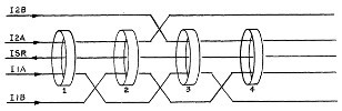 about 2 cubic feet
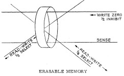 Common:
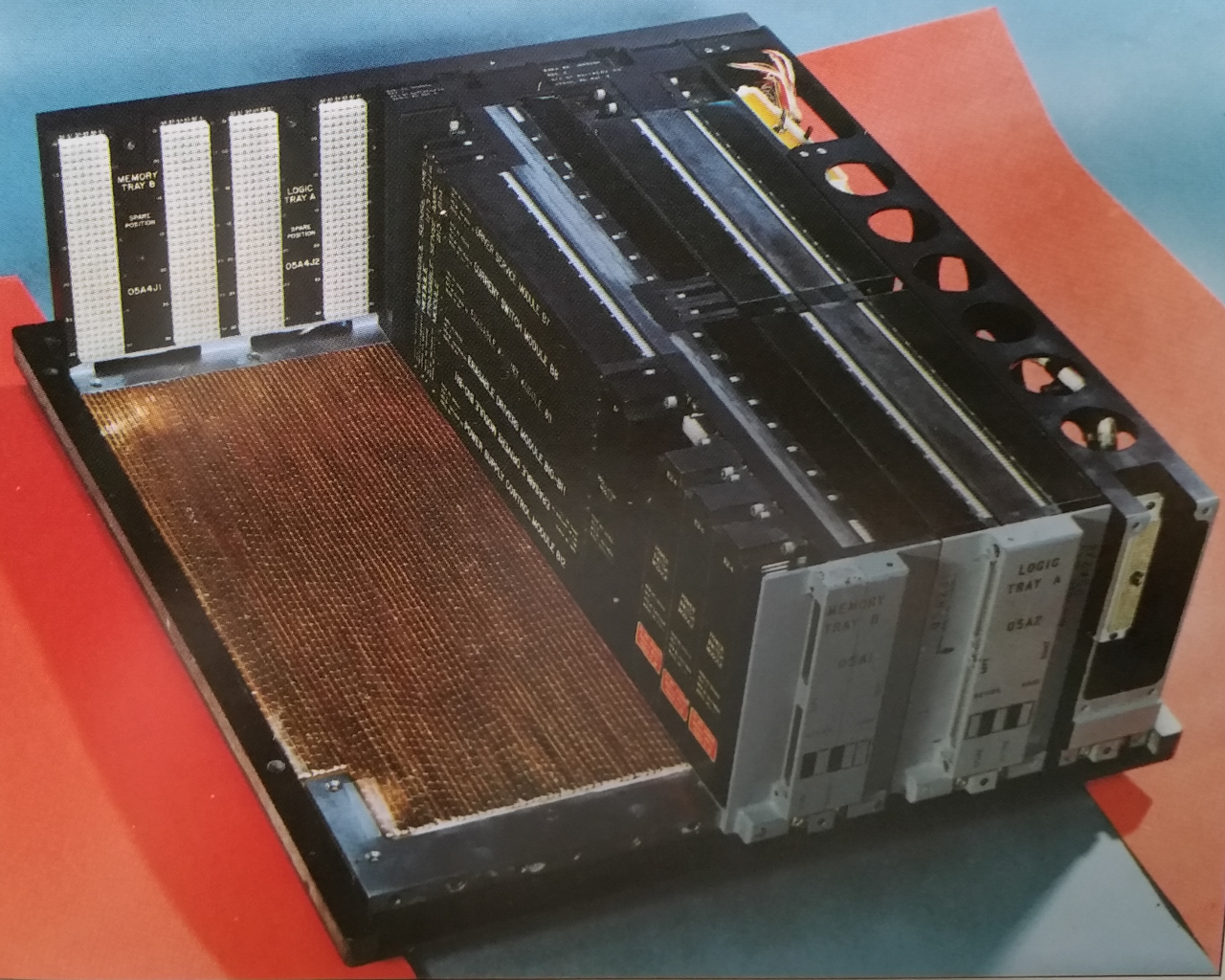
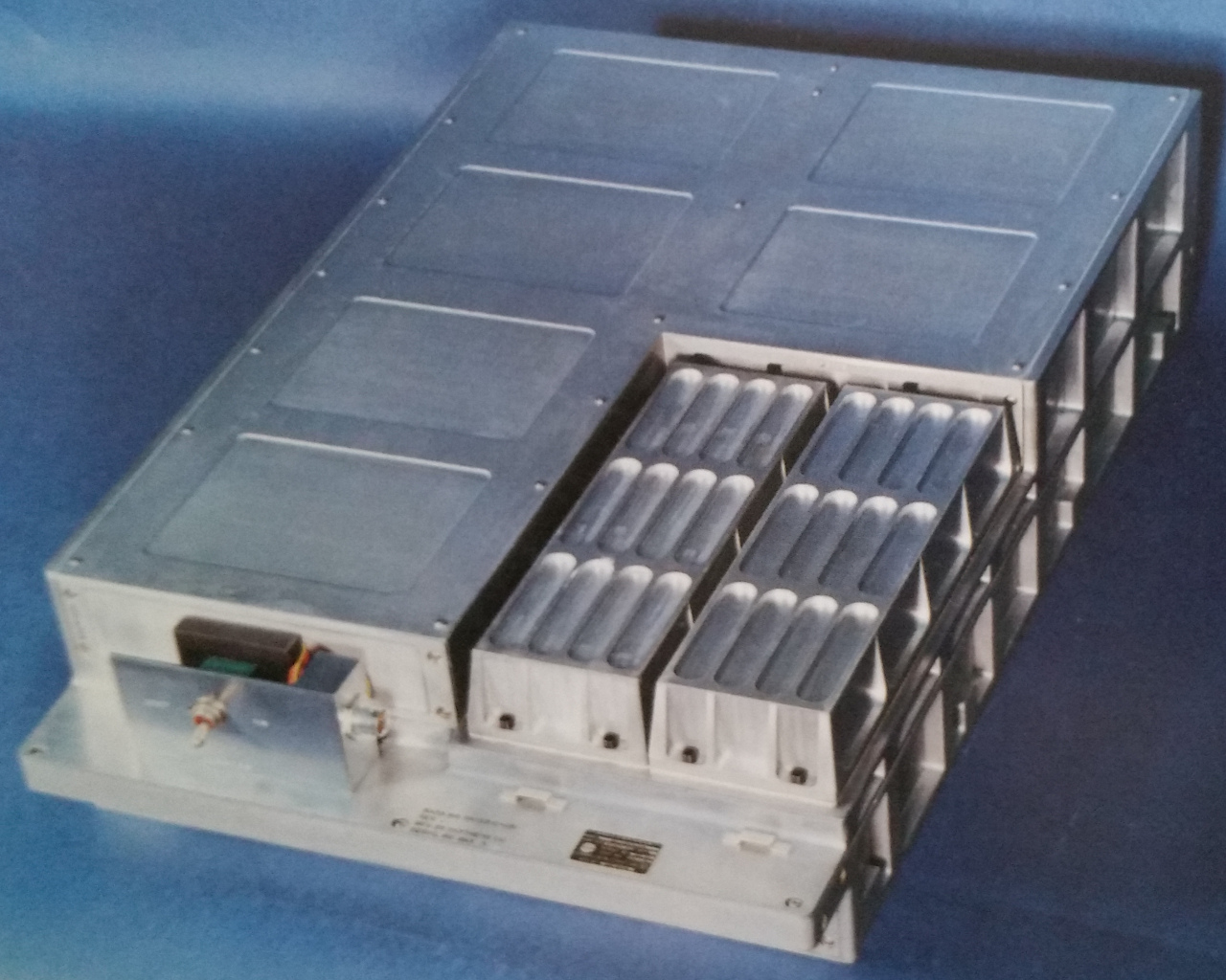
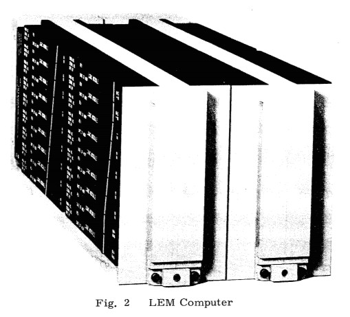
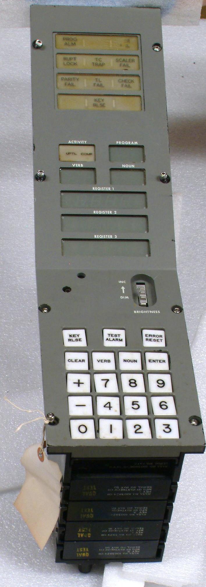

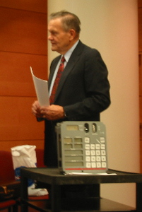 The left-hand picture above is a
nav-bay DSKY. On the right is a photo of a main control-panel
DSKY.
The left-hand picture above is a
nav-bay DSKY. On the right is a photo of a main control-panel
DSKY.
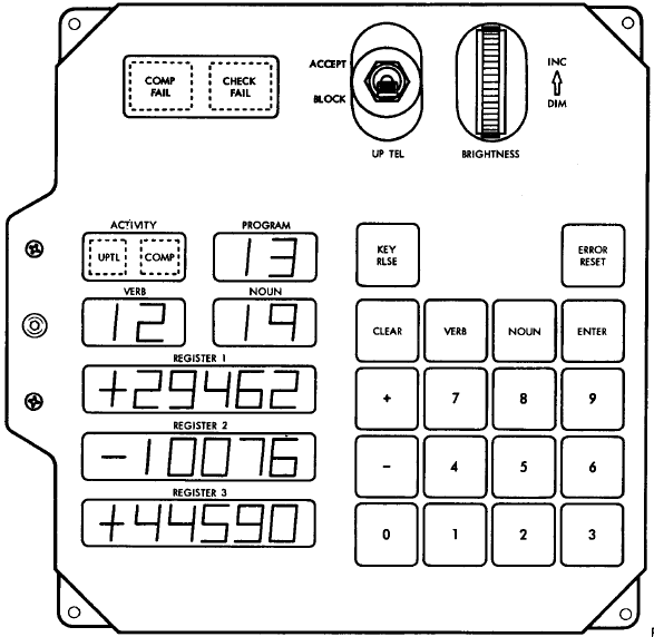
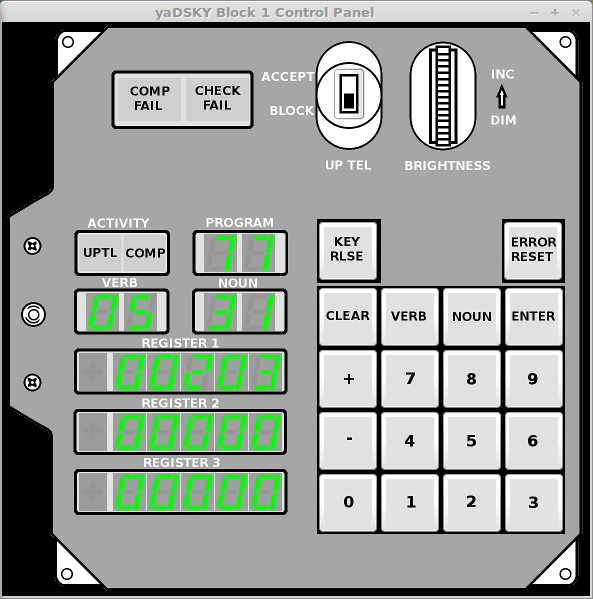
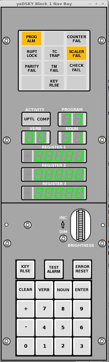

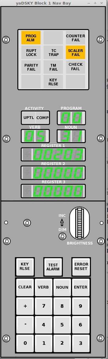
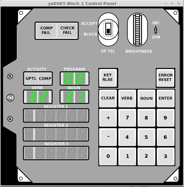
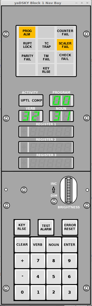
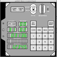
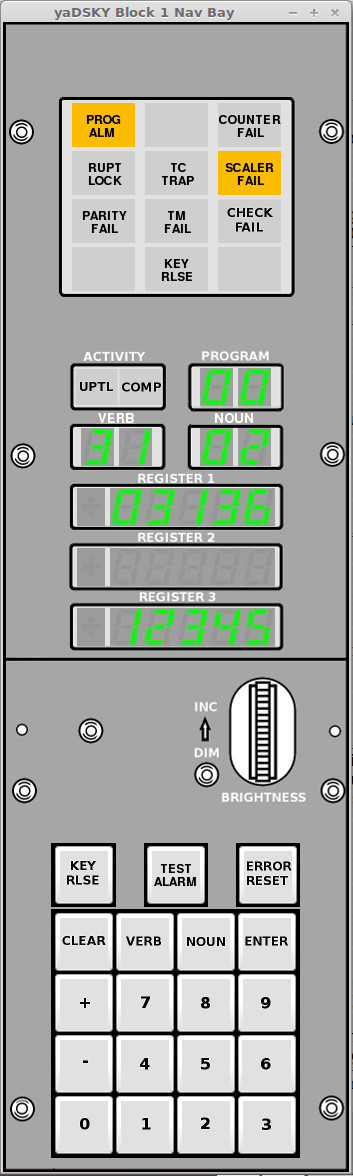


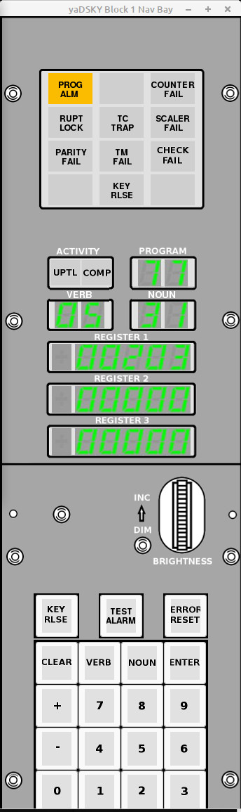
